Download
1 / 10
110 likes | 304 Views
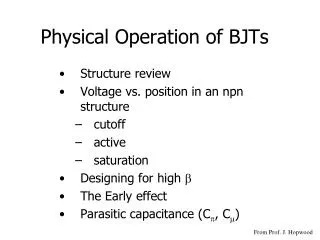
Physical Operation of BJTs. Structure review Voltage vs. position in an npn structure cutoff active saturation Designing for high b The Early effect Parasitic capacitance (C p , C m ). From Prof. J. Hopwood. E. B. C. metal silicon oxide doped silicon wafer (chip). npn structure.

E N D
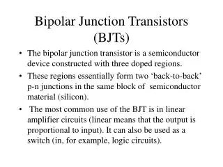
Physical Operation of BJTs Structure review Voltage vs. position in an npn structure cutoff active saturation Designing for high b The Early effect Parasitic capacitance (Cp, Cm) From Prof. J. Hopwood
E B C metal silicon oxide doped silicon wafer (chip) npn structure integrated circuit BJT The npn Bipolar Junction Transistor n-type p-type n+-type collector emitter base
n C p B n+ E - - + + - - + + - - + + Voltage inside the npn structure V(x) ~0.7 volts (for Si) x EBJ=off CBJ=off At zero bias (vBE=0, vBC=0), currents balanced, no net current flow iB =iC = 0 (cutoff)
n (C) p (B) n+ (E) - - + + - - + + - - + + Voltage inside the npn structure V(x) iB ~0.7 volts (for Si) -iE>>iB x EBJ=on CBJ=off When (vBE=0.65, vC>vB) electrons and holes overcome the built-in voltage barrier between the base and emitter iB > 0 and iE > iB (due to n+ emitter doping)
n (C) p (B) n+ (E) - - + + - - + + - - + + Voltage inside the npn structure V(x) iB vC -iC ~0.7 volts (for Si) -iE>>iB x EBJ=on CBJ=off If the base region is very thin, the electrons injected by the emitter are collected by the positive voltage applied at vC iC iE>>iB (active region)
n (C) p (B) n+ (E) - - + + - - + + - - + + Voltage inside the npn structure V(x) iB vC iC ~0.7 volts (for Si) iE>>iB x CBJ=off EBJ=on If the base region is too thick, the electrons injected by the emitter are lost by recombining with holes in the base before the voltage applied at vC can collect them (another component of base current): iC < iE (active region with low a, b)
n (C) p (B) n+ (E) - - + + - - + + - - + + Voltage inside the npn structure V(x) iB vC -iC -iE>>iB x -iB CBJ=on EBJ=on If vC drops such that the CBJ is forward biased, the collector no longer is able to gather the injected electrons! These uncollected electrons exit through the base! iB is large and iC is small Saturation
How do we achieve high b? • make the base region thin (typ. <1 micron) • this makes the collection efficiency of injected electrons high and decreases the chance of these electrons recombining in the base region • make the emitter heavily doped • iE/iB n(emitter)/p(base) • (emitter doping concentration)/(base doping conc.) These two quantities are difficult to control precisely! Therefore, the current gain is not uniform among BJTs (except when the BJTs are all made on the same chip... an integrated circuit)
n (C) p (B) n+ (E) - - - - + + + + - - - - + + + + - - - - + + + + The Early Effect • As VC increases, the depletion width of the B-C junction becomes wider. • This make the base width more narrow • This increases the collection efficiency • Finally, iC/iB increases (higher ) n (C) p (B) n+ (E) IC VCE
n (C) p (B) n+ (E) - - + + - - + + - - + + Cm Cp Parasitic (unwanted) Capacitance • Each junction forms a parasitic capacitor: semiconductor/depletion/semiconductor Cm Cp At high frequency, (1/jwC 0), these capacitors become short circuits and prevent the BJT from proper operation. This is a fundamental limit on high frequency circuits.