Download
1 / 53
530 likes | 732 Views
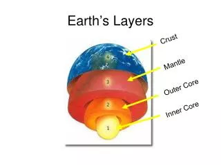
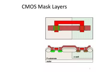
n well. P substrate. wafer. CMOS Mask Layers. Why we need design rules. Masks are tooling for manufacturing. Manufacturing processes have inherent limitations in accuracy. Design rules specify geometry of masks which will provide reasonable yields.

E N D
n well P substrate wafer CMOS Mask Layers
Why we need design rules • Masks are tooling for manufacturing. • Manufacturing processes have inherent limitations in accuracy. • Design rules specify geometry of masks which will provide reasonable yields. • Design rules are determined by experience.
Manufacturing problems • Photoresist shrinkage, tearing. • Variations in material deposition. • Variations in temperature. • Variations in oxide thickness. • Impurities. • Variations between lots. • Variations across a wafer.
Mask misalignment • Dust • Process parameters (e.g., lateral diffusion) • Rough surfaces
mask misaligned 0.3 both materials Contact: 0.44 x 0.44 0.14
Transistor problems • Varaiations in threshold voltage: • oxide thickness; • ion implanatation; • poly variations. • Changes in source/drain diffusion overlap. • Variations in substrate.
Wiring problems • Diffusion: changes in doping -> variations in resistance, capacitance. • Poly, metal: variations in height, width -> variations in resistance, capacitance. • Shorts and opens:
Oxide problems • Variations in height. • Lack of planarity -> step coverage. metal 2 metal 2 metal 1
Via problems • Via may not be cut all the way through. • Undesize via has too much resistance. • Via may be too large and create short.
Rule for various layers – of IC fabrication • (0.3µ) 1.Well 2.Active 3.Poly 4.Select 5.Poly Contact 6.Active Contact 7.Metal-1 8.Via 9.Metal-2 10.Via2 11.Metal-3
Rules for Well – 0.3 µ Minimum width 3.5µ Minimum spacing between 5.4 µwells at different potential Minimum spacing between 1.8µwells at same potential