Appendix A – Part 2: Logic Circuits
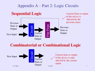
Previous State or Output. Previous State or Output. Circuit. Flip Flops. Current State or Output. New Input. Circuit. New Input. Current State or Output. Appendix A – Part 2: Logic Circuits. Sequential Logic. Current State or output of the device is affected by the previous states.

Appendix A – Part 2: Logic Circuits
E N D
Presentation Transcript
Previous State or Output Previous State or Output Circuit Flip Flops Current State or Output New Input Circuit New Input Current State or Output Appendix A – Part 2: Logic Circuits Sequential Logic Current State or output of the device is affected by the previous states Combinatorial or Combinational Logic Current State or output of the device is only affected by the current inputs Lecture
Previous State or Output Previous State or Output Circuit Flip Flops Current State or Output New Input Appendix A – Part 2: Logic Circuits Notice how the output feeds the input • S and R stand for set and reset respectively • constructed from a pair of cross-coupled NOR gates • the stored bit is present on the output marked Qa • If S and R inputs are both low, maintains the Qa and Qb in constant state, • If S (Set) is pulsed high while R is held low, then the Qa output is forced high,and stays high even after S returns low; • if R (Reset) is pulsed high while S is held low, then the Qa output is forced low, and stays low even after R returns low. Lecture
Gated SR Latch or Flip Flop • The time at which the latch is SET or RESET is controlled by a CLOCK input • Called Gated SR Latch Lecture
Gated SR Latch built using NAND Lecture
Gated D Latch • Inputs S and R are derived from a single input D • Clock pulse controls when the output is triggered • Samples the D input at the time the clock is HIGH and stores that info until the next clock pulse Lecture
Potential Problem • Thus far, the assumption has been the inputs S and R (or D) not changing while CLK is HIGH • What would happen if S, R and/or D changed ? The output would change immediately • This could be a problem • To fix this (next ppt) Lecture
Master-Slave Flip Flop Master Slave Q Q m s D D Q D Q Q Clock Clk Q Clk Q Q Use 2 D flip flops – Master – Slave – the Slave’s clock is set to zero – therefore, if there was a change in the Master’s input, D, it wouldn’t effect the slave’s Q value – the slave holds the value (a) Circuit Clock D Q m Q = Q s (b) Timing diagram Clock’s negative edge causes change • If D changes while Master CLK is HIGH, Qm changes immediately - Qs stays the same because Slave CLK=0 • Once the CLK goes LOW, Slave FF reacts because its CLK=1 – so it thens reflects D Q D The arrow only symbolizes “positive edge” clock - the arrow with the NOT symbolizes “negative edge” clock Q (c) Graphical symbol Figure A.28.Master-slave D flip-flop. Lecture
T Flip Flop T Flip Flops are good for counters – changes its state every clock cycle, if the input, T, is 1 • Positive-edge triggered flip flop • Since the previous state of Q was 0, it complements it to 1 Lecture
JK Flip Flop Combines the behavior of the SR and T flip flops • First three entries are the same behavior as the SR Latch (when CLK=1) • Usually the state S=R=1 undefined – for the JK Flip Flop, for J=K=1, next state is the complement of the present state Can store data like a D Flip Flop or can tie J & K inputs together and use to build counters (like a T flip flop) Lecture
Registers and Shift Registers A Flip Flop can store ONE bit – in being able to handle a WORD, you will need a number of flip flops (32, 64, etc) arranged in a common structure called a REGISTER. • All flip flops are synchronized by a common clock • Data written into (loaded) flip flops at the same time • Data is read from all flip flops at the same time F F F F 1 2 3 4 In Out D Q D Q D Q D Q Clock Q Q Q Q Figure A.33. A simple shift register. • Want the ability to rotate and shift the data • Clock pulse will cause the contents of F1, F2, F3 and F4 to shift right (serially) • To do a rotation, simply connect OUT to IN Lecture
Registers and Shift Registers • Can load either serially or in parallel • When clock pulse occurs, • Serial shift takes place if Shift’/Load=0 or • if Shift’/Load=1, parallel load is performed Lecture
Counters • 3-stage or 3-bit counter constructed using T Flip Flops • With T Flip Flips, when input T=1, the flip flop toggles – changes state for each successive clock pulse • Initially all set to 0 • When clock pulse, Q0=1, therefore Q’=0 disabling Q1 and Q1 disables Q2 (have 1,0,0) • For the 2nd clock pulse, Q0=0, therefore Q’=1, causing Q1=1 and therefore Q’=0 disabling Q2 (have 0,1,0) • For the 3rd clock pulse, Q0=1, therefore Q’=0 disabling Q2 and therefore disabling Q3 (have 1,1,0) • Etc…. LSB 000 001 010 011 100 101 110 111 Hmmm Lecture Called a Ripple Counter
Decoders Example – encoded message 01 means 2 Output - Decoded message Input - Encoded message Lecture
Decoders – another example Lecture
Multiplexers Depending the “select input” combination, 1 of 4 data inputs is chosen for output Explain how you rotate here to get different info coming out the mux Example – if “select input” 10 is realized, data input on X3 is displayed as output, Z Lecture
Multiplexers Can also use multiplexers to implement logic functions Given this truth table, group X1,X2 being 00, 01, 10 and 11 – notice what happens with X3 • 3-input truth table can be done with a 4-input mux • 4-input truth table can be done with a 8-input mux • 5-input truth table can be done with a 16-input mux • Etc.. Lecture