Download
1 / 17
170 likes | 364 Views
A Novel Method to Measure the Absolute Value of the Magnetic Penetration Depth in Superconductors. Vladimir V. Talanov*, Steven M. Anlage , Lucia Mercaldo # John H. Claassen (NRL). * Solid State Measurements, Inc., Pittsburgh, PA # ENEA- Portici Research Center - Italy .

E N D
A Novel Method to Measure the Absolute Value of the Magnetic Penetration Depth in Superconductors Vladimir V. Talanov*, Steven M. Anlage, Lucia Mercaldo# John H. Claassen (NRL) * Solid State Measurements, Inc., Pittsburgh, PA # ENEA- Portici Research Center - Italy RF Superconducting Materials Workshop at Fermilab
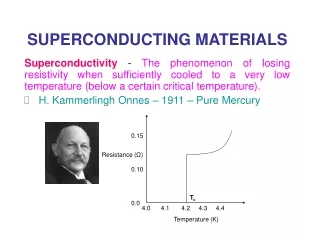
Motivation Measurement of l gives insight into material properties and quality • varies with ℓMFP, magnetic field (non-linear Meissner effect), direction, weak links, etc. Most techniques measure Dl, but not the absolute magnitude of l H(y) vacuum superconductor l y Typicallyl ~ 15 nm to 10’s of mm
4 Classes of Techniques to Measure l • Absolute Length Scale Techniques • Meissner state flux exclusion. One sample dimension (L) is known • df ~ (L – g dl) x (area of the sample) • (empty vs. pertubed) The Variable-Spacing Parallel Plate Resonator l/L ~ 10-1 and systematically larger Problem: often l / L ~ 10-3 - 10-4 l(0) found from fitting dl(T) to theory • 2) Reflection / Transmission • Mutual inductance of two coils • Microwave transmission • “Missing area” sum-rule, KK analysis Problems: requires large (~cm2) thin films Requires very accurate spectroscopy • 3) Probes of Internal Magnetic fields • mSR • Polarized Neutron Reflectometry Problems: very specialized techniques Requires model of mixed state or very flat large area surfaces • 4) Josephson Tunneling • Magnetic diffraction pattern Problem: requires creating a tunnel junction
The Variable-Spacing Parallel Plate Resonator Vary s s: contact – ~ 100 mm in steps of 10 nm to 1 mm Principle of Operation: Measure the resonant frequency, f0, and the quality factor, Q, of the VSPPR versus the continuously variable thickness of the dielectric spacer (s), and to fit them to theoretical forms in order to extract the absolute values of l and Rs. The measurements are performed at a fixed temperature In our experiments L, w ~ 1 cm
The VSPPR Experiment Films held and aligned by two sets of perpendicular sapphire pins Dielectric spacer thickness (s) measured with capacitance meter
VSPPR: Theory of Operation Superconducting samples Resonant Frequency Quality Factor fringe effect SC Trans. line resonator f* is a reference frequency Assumes: 2 identical and uniform films, local electrodynamics, Rs(f) ~ f2 V. V. Talanov, et al., Rev. Sci. Instrum. 71, 2136 (2000) US Patent # 6,366,096
High-Tc Superconducting Thin Films at 77 K Mutual Inductance Measurements l fit: 257 ± 25 nm (l1+l2)/2 = 300 ± 15 nm Rs fit: 200 ± 20mW @ f* = 10 GHz L = 9.98 mm, w = 9.01 mm, film thickness d = 760 ± 30 nm, Tc = 92.4 K
VSPPR: Theory of Operation Normal Metal samples Resonant Frequency Quality Factor fringe effect NM Trans. line resonator Assumes: 2 identical and uniform films, local electrodynamics, Rs(f) ~ f1/2 V. V. Talanov, et al., Rev. Sci. Instrum. 71, 2136 (2000) US Patent # 6,366,096
Thick Copper Plates at Room Temperature f0(s) f0(s) Q(s) Q(s) dskin fit (f* = 10 GHz): 0.79 ± 0.1mm (from f-fit) and 0.77 ± 0.1 mm (from Q-fit) Theory: rCu = 1.7 mWcm at 293 K, yielding dskin = 0.68 mm (f* = 10 GHz) L = 11.97 mm, w = 9.88 mm, plate thickness d = 0.7 mm
What Relevance for SRF? The VSPPR could act as a scanned probe for l(x, y) on Nb sheets The “probe” film is a known reference standard Compare dskin(300 K) to l(1.8 K) Correlate with surface analysis probe film Nb Sheet Employ different modes of the VSPPR to study lk direction-dependence of ns/m tensor Vortex generation at defects at high powers Build conformal probe/reference films for investigation of d(r, f, z) and l(r, f, z) of finished cavities Design new reference resonator structures (sphere, cylinder, ray-chaotic, …)
Conclusions The VSPPR offers the opportunity to measure the absolute screening length scale both in the normal and superconducting states The results have been validated with alternative data The VSPPR also provides the absolute surface resistance The VSPPR can be employed as a scanned probe of Nb surface properties For more information and details, see: V. V. Talanov, et al., Rev. Sci. Instrum. 71, 2136 (2000) US Patent # 6,366,096
Details Requirement of an offset spacing s0: s = sc + s0 Tilting of the plates: Measured to be less than 1 mrad Misalignment of the plates Measurement of low-Q resonant open-resonator modes Background subtraction Effect of non-flatness of the plates Secondary fitting parameters V. V. Talanov, et al., Rev. Sci. Instrum. 71, 2136 (2000) US Patent # 6,366,096
Questions to be addressed RF / Superconducting properties Coupling with surface analysis! Is the comparison Samples/Cavities relevant? What is the link between DC/RF properties, between low field/high field properties? Are there other parameters “easy” to measure that could give us better prediction of the cavity behavior? Thermal transfer: influence of annealing, grain boundaries….
Capacitance Measurement of s In-situ Capacitance Measurements C-meter 50-m-thick Au wires In pads Cu (HTS) films
Rs--Standard for Characterization of Superconducting Materials for Microwave Applications Proposed definition for Rsvia the well-standardized quantities -- frequency and length: Effective Surface Resistance of 100 at 10 GHz is a FWHM = 2.533 MHz of the resonance curve for the Ohmic Q-factor produced by the VSPPR with the effective dielectric spacer thickness seff = s+ 2eff = 10 m
Experimental Setup:Variable PPR Differential Micrometer Head, 70 nm resolution Actuator Displacement Sensor, 25 nm resolution Sensor target: front mirror Top flexure Be/Cu bearing 1 mm fine travel Coaxial thin wall ss tubes Slider 12 “ Bottom flexure Be/Cu bearing Flexible clamps for top & bottom HTS films LN2 PPR with 0-200 m Variable Dielectric Spacer filled by LN2 Films Aligner Bottom film’s substrate Top film’s substrate Al pins Antenna loops Top view Coupling probes Coax cables IN OUT