Solar Cell Technology
Solar Cell Technology. Engineering 10 October 11, 2007 Professor Richard Chung Department of Chemical and Materials Engineering San Jose State University San Jose, California 95192-0082 (408) 924-3927, w.richard.chung@sjsu.edu. What is a Solar Cell?.

Solar Cell Technology
E N D
Presentation Transcript
Solar Cell Technology Engineering 10 October 11, 2007 Professor Richard ChungDepartment of Chemical and Materials Engineering San Jose State University San Jose, California 95192-0082 (408) 924-3927, w.richard.chung@sjsu.edu
What is a Solar Cell? • It is also known as Photovoltaic cell (PV cell) • A device that converts light energy (solar energy) directly to electricity. • The term solar cell is designated to capture energy from sunlight, whereas PV cell is referred to an unspecified light source. • It is like a battery because it supplies DC power. • It is not like a battery because the voltage supplied by the cell changes with changes in the resistance of the load. Made from a single crystalline silicon wafer
History • The photovoltaic effect was first recognized in 1839 by French physicist Alexandre-Edmond Becquerel. However, it was not until 1883 that the first solar cell was built, by Charles Fritts, who coated the semiconductor selenium with an extremely thin layer of gold to form the junctions. The device was only around 1% efficient. • Russell Ohl patented the modern solar cell in 1946 (U.S. Patent 2,402,662)
Applications of Solar Cells • Renewable energy • Can be powered for remote locations • It’s free, limitless, and environmentally friendly…
Semiconductor material can be p-type (hole carriers) or n-type (electron carriers) N-type has impurities with an extra electron (phosphorus) P-type has impurities with one fewer electron (boron) Put them together: p-n junction A solar cell is a very large p-n junction (or diode) B- P+ n-type p-type Physics of Solar Cells
The holes from the p-type side diffuse to the n-type side. The electrons diffuse to the p-type side. This leaves behind charged ions (missing electrons or holes). e B- P+ n-type h p-type Basic Physics of Solar Cells
n-type p-type P+ B- P+ B- P+ B- E-field Built-In Electric Field • The charged atoms (ions) create an electric field. • This electric field makes it easy for current to flow in one direction, but hard to flow in the opposite direction.
Light breaks silicon bonds and creates “free” electrons and holes “missing electrons” Holes are positive charges Built-in field separates electrons and holes n-type p-type P+ B- P+ e B- h P+ B- E-field Generating Charges From The Sun
Connect diode to a circuit Photocurrent goes through resistor Causes a voltage drop n-type p-type P+ B- P+ e B- h B- P+ E-field V=IR Generating Charges From The Sun IPC
Forward biases the diode Causes a current in opposite direction n-type p-type +V -V h P+ B- e P+ B- IFB P+ B- V=IR IPC Generating Charges From The Sun
If R is very large, V is very large If V is very large, IFB = IPC I=0 Open Circuit condition n-type p-type P+ B- P+ B- P+ B- Generating Charges From The Sun +V -V h e IFB=IPC V=IR IPC
If R is very small, V is very small If V = 0, IFB = 0 I= IPC Short Circuit condition n-type p-type P+ B- P+ B- P+ B- Generating Charges From The Sun +V -V h e IFB=0 V=IR=0 IPC
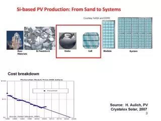
Construction of Solar cells • They are constructed by layering special materials called semiconductors into thin, flat sandwiches. • These are linked by electrical wires and arranged on a panel of a stiff, non-conducting material such as glass. The panel itself is called a module. • Modules are then interconnected, in series or parallel, or both, to create an array with the desired peak DC voltage and current. http://www.specmat.com/Overview%20of%20Solar%20Cells.htm
a. Encapsulate b. Contact Grid c. Antireflective Coating d. N-type Silicon e. P-type Silicon f. Back Contact
How Solar cells work • Function 1: Photogeneration of charge carriers (electrons and holes) in a light-absorbing material • Function 2: Separation of the charge carriers to a conductive medium such as a metal contact or a wire in order to transmit the electricity • It supplies a voltage and a current to a resistive load (light, battery, motor). • Power = Current x Voltage
The photons (yellow dot) carry their energy down through the cell. The photons give up their energy to electrons (green dot) in the lower, p-type layer. The electrons use this energy to jump across the barrier into the upper, n-type layer and escape out into the circuit. Flowing around the circuit, the electrons make the lamp light up. 1. A solar cell is a sandwich of n-type silicon (blue) and p-type silicon (red). 2. When sunlight shines on the cell, photons (light particles) bombard the upper surface. http://www.explainthatstuff.com/solarcells.html
Solar Cell Properties • Open circuit voltage (VOC) • Short circuit current (ISC) • Maximum power • Efficiency Factors affecting Solar Cell Performance • Light intensity (type of light) • Light wavelength (color of light) • Angle of incident light • Surface condition of solar cells (cleanness) • Temperature on solar cells
Peak Power Point (Maximum Power) • A solar cell may operate over a wide range of voltages (V) and currents (I). By increasing the resistive load on an irradiated cell continuously from zero (a short circuit) to a very high value (an open circuit) one can determine the maximum-power point, the point that maximizes V×I, that is, the load for which the cell can deliver maximum electrical power at that level of irradiation. • Dynamically adjust the load so the maximum power is always transferred, regardless of the variation in lighting.
Efficiency • A solar cell's energy conversion efficiency(η, "eta"), is the percentage of power converted (from absorbed light to electrical energy) and collected, when a solar cell is connected to an electrical circuit. This term is calculated using the ratio of Pm, divided by the input light irradiance under "standard" test conditions (E, in W/m²) and the surface area of the solar cell (Ac in m²).
Solar Cell Process Flow • Start with n-type silicon wafers • Cleaning the wafers Sulfuric: peroxide - removes organics Buffered Hydrofluoric acid - removes residual oxide HCl: peroxide - removes heavy metals • Spin on dopant: a liquid source of boron (p-type impurity) • Anneal: 1000oC furnace step drives B into wafer (forming diode).
Solar Cell Process Flow • Metallization: Aluminum deposited on the front and backside of the wafer. • Patterning: Resist is spun on the front and back sides of the wafer and exposed using a mask and UV light. The exposed resist is removed during developing. • Metal Etch: The pattern from the mask is transferred to the metal using a wet metal etch. The remaining photoresist is then removed. • Metal Anneal: The wafer is annealed at 400C to improve the conductivity of the metal.
MASK LEVEL 1 Semiconductor Light from aligner Positive photoresist Semiconductor
N- Type Silicon P-Type Silicon Metal P-type Metallization (Al) Boron Diffusion (P-Type) N-type
To make your own solar cells • MatE 153 – Electronic Materials Properties • MatE/EE 129 - Basic IC Processing • MatE/ChE 166 - Advanced Thin Film Processes • MatE/EE 167 - Microelectronics Manufacturing Methods • Major/Minor in Materials Engineering • Dr. Emily Allen of Chemical and Materials Engineering and Dr. David Parent of Electrical Engineering
Efficiency vs. cost Solar cell efficiencies vary from 6% for amorphous silicon-based solar cells to 42.8% with multiple-junction research lab cells. Solar cell energy conversion efficiencies for commercially available multicrystalline Si solar cells are around 14-16%. The highest efficiency cells have not always been the most economical — for example a 30% efficient multijunction cell based on exotic materials such as gallium arsenide or indium selenide and produced in low volume might well cost one hundred times as much as an 8% efficient amorphous silicon cell in mass production, while only delivering about four times the electrical power. Current Obstacles
Future Developments • The first generation photovoltaic, consists of a large-area, single layer p-n junction diode, which is capable of generating usable electrical energy from light sources with the wavelengths of sunlight. These cells are typically made using a silicon wafer. • The second generation of photovoltaic materials is based on the use of thin-film deposits of semiconductors. These devices were initially designed to be high-efficiency, multiple junction photovoltaic cells.
Third generationphotovoltaics are very different from the previous semiconductor devices as they do not rely on a traditional p-n junction to separate photogenerated charge carriers. These new devices include photoelectrochemical cells, polymer solar cells, and nanocrystal solar cells. Dye-sensitized solar cells are now in production. Examples include Amorphous silicon, Polycrystalline silicon, micro-crystalline silicon, Cadmium telluride, copper indium selenide/sulfide. • Fourth generation Composite photovoltaic technology with the use of polymers with nano particles can be mixed together to make a single multispectrum layer. Then the thin multi spectrum layers can be stacked to make multispectrum solar cells more efficient and cheaper based on polymer solar cell and multi junction technology used by NASA on Mars missions.
Review Question 1 A solar cell is designated to capture energy from: • Sunlight • White light • Incandescent light • Halogen light • All of the above
Review Question 2 A P-type semiconductor is a ________ carrier? • Photon • Electron • Hole • Ion • None of the above
Review Question 3 Which of the following is NOT a property of a solar cell? • Open circuit voltage (VOC) • Short circuit current (ISC) • Resistor in the circuit • Maximum power • Efficiency
Review Question 4 Which of the following will impair a solar cell’s performance? • Size of the cell • A water stain • Shape of the cell • All of the above • None of the above
Review Question 5 What is the challenge in solar cell development? • Cost • Maximum power • Efficiency • New thin film material • All of the above