Download
1 / 22
220 likes | 239 Views
Explore the fundamental building blocks of computer memory systems, from datapath components to memory hierarchy. Delve into concepts such as primary and secondary memory, caches, registers, control units, and more. Learn how memory systems optimize speed, capacity, and cost efficiency. This overview covers various aspects, including memory types, architecture, components, and advantages. Understand the design and functioning of memories like ROM, SRAM, and DRAM. Gain insights into memory timing definitions, memory configurations, and techniques to reduce delays in word and bit lines for efficient memory operations.

E N D
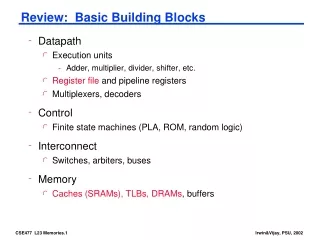
Review: Basic Building Blocks • Datapath • Execution units • Adder, multiplier, divider, shifter, etc. • Register file and pipeline registers • Multiplexers, decoders • Control • Finite state machines (PLA, ROM, random logic) • Interconnect • Switches, arbiters, buses • Memory • Caches (SRAMs), TLBs, DRAMs, buffers
A Typical Memory Hierarchy • By taking advantage of the principle of locality: • Present the user with as much memory as is available in the cheapest technology. • Provide access at the speed offered by the fastest technology. On-Chip Components Control eDRAM Secondary Memory (Disk) Instr Cache Second Level Cache (SRAM) ITLB Main Memory (DRAM) Datapath Data Cache RegFile DTLB Speed (ns): .1’s 1’s 10’s 100’s 1,000’s Size (bytes): 100’s K’s 10K’s M’s T’s Cost: highest lowest
m bits m bits S0 S0 Word 0 Word 0 S1 S1 Word 1 Word 1 S2 S2 Word 2 Storage Cell A0 Word 2 Storage Cell S3 S3 A1 Decoder n words Ak-1 Sn-2 Sn-2 Word n-2 Word n-2 Sn-1 Sn-1 Word n-1 Word n-1 Input/Output Input/Output 1D Memory Architecture n words n select signals Decoder reduces # of inputs k = log2 n
2D Memory Architecture bit line 2k-j word line Aj Aj+1 Row Address storage (RAM) cell Row Decoder Ak-1 m2j Column Address A0 selects appropriate word from memory row A1 Column Decoder Aj-1 Sense Amplifiers amplifies bit line swing Read/Write Circuits Input/Output (m bits)
3D Memory Architecture Row Addr Column Addr Block Addr Input/Output (m bits) Advantages: 1. Shorter word and/or bit lines 2. Block addr activates only 1 block saving power
Precharged MOS NOR ROM Vdd 0 1 precharge WL(0) GND 0 1 WL(1) WL(2) GND WL(3) BL(0) BL(1) BL(2) BL(3) 1 1 1 1 0 1 1 0
MOS NOR ROM Layout Metal1 on top of diffusion WL(0) GND (diffusion) WL(1) Basic cell 10 x 7 Metal1 Polysilicon WL(2) GND (diffusion) WL(3) BL(0) BL(1) BL(2) BL(3) Only 1 layer (contact mask) is used to program memory array, so programming of the ROM can be delayed to one of the last process steps.
Transient Model for NOR ROM precharge metal1 rword BL poly Cbit WL cword Word line parasitics Resistance/cell: 35 Wire capacitance/cell: 0.65 fF Gate capacitance/cell: 5.10 fF Bit line parasitics Resistance/cell: 0.15 Wire capacitance/cell: 0.83 fF Drain capacitance/cell: 2.60 fF
Propagation Delay of NOR ROM • Word line delay • Delay of a distributed rc-line containing M cells tword = 0.38(rword x cword) M2 = 20 nsec for M = 512 • Bit line delay • Assuming min size pull-down and 3*min size pull-up with reduced swing bit lines (5V to 2.5V) Cbit = 1.7 pF and IavHL = 0.36 mA so tHL = tLH = 5.9 nsec
Read-Write Memories (RAMs) • Static – SRAM • data is stored as long as supply is applied • large cells (6 fets/cell) – so fewer bits/chip • fast – so used where speed is important (e.g., caches) • differential outputs (output BL and !BL) • use sense amps for performance • compatible with CMOS technology • Dynamic – DRAM • periodic refresh required • small cells (1 to 3 fets/cell) – so more bits/chip • slower – so used for main memories • single ended output (output BL only) • need sense amps for correct operation • not typically compatible with CMOS technology
Memory Timing Definitions Read Cycle Read Read Access Read Access Write Cycle Write Write Hold Write Setup Data Data Valid
4x4 SRAM Memory read precharge 2 bit words bit line precharge enable WL[0] !BL BL A1 WL[1] Row Decoder A2 WL[2] WL[3] Column Decoder A0 clocking and control sense amplifiers write circuitry BL[i] BL[I+1]
2D Memory Configuration Sense Amps Sense Amps Row Decoder
driver driver polysilicon word line WL metal word line polysilicon word line WL metal bypass Decreasing Word Line Delay • Drive the word line from both sides • Use a metal bypass • Use silicides
Decreasing Bit Line Delay (and Energy) • Reduce the bit line voltage swing • need sense amp for each column to sense/restore signal • Isolate memory cells from the bit lines after sensing (to prevent the cells from changing the bit line voltage further) - pulsed word line • generation of word line pulses very critical • too short - sense amp operation may fail • too long - power efficiency degraded (because bit line swing size depends on duration of the word line pulse) • use feedback signal from bit lines • Isolate sense amps from bit lines after sensing (to prevent bit lines from having large voltage swings) - bit line isolation
Pulsed Word Line Feedback Signal • Dummy column • height set to 10% of a regular column and its cells are tied to a fixed value • capacitance is only 10% of a regular column Read Word line Bit lines Dummy bit lines Complete 10% populated
Pulsed Word Line Timing • Dummy bit lines have reached full swing and trigger pulse shut off when regular bit lines reach 10% swing Read Complete Word line V = 0.1Vdd Bit line V = Vdd Dummy bit line
Bit Line Isolation bit lines V = 0.1Vdd isolate Read sense amplifier sense V = Vdd sense amplifier outputs
6-transistor SRAM Cell WL M2 M4 Q M6 M5 !Q M1 M3 !BL BL