pn Junction Electrostatics in Semiconductor Devices
230 likes | 256 Views
Exploring the physics of pn junction electrostatics, Poisson's equation, energy band diagrams, and depletion approximation for charge distribution. Learn about Vbi, depletion layer width, and bias effects on electrostatics.

pn Junction Electrostatics in Semiconductor Devices
E N D
Presentation Transcript
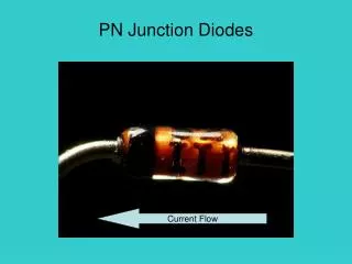
Semiconductor Device Physics Chapter 5 pn Junction Electrostatics
Chapter 5 pn Junction Electrostatics Metallurgical Junction • Doping profile Step junction idealization
Chapter 5 pn Junction Electrostatics Poisson’s Equation • Poisson’s equation is a well-known relationship in electricity and magnetism. • It is now used because it often containsthe starting point in obtaining quantitative solutions for the electrostatic variables. • In one-dimensional problems, Poisson’s equation simplifies to:
Chapter 5 pn Junction Electrostatics Equilibrium Energy Band Diagram • pn-Junction diode
Chapter 5 pn Junction Electrostatics Qualitative Electrostatics • Equilibrium condition Band diagram Electrostatic potential
Chapter 5 pn Junction Electrostatics Qualitative Electrostatics • Equilibrium condition Electric field Charge density
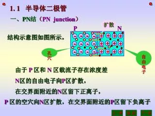
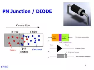
Chapter 5 pn Junction Electrostatics Formation of pn Junction and Charge Distribution – + qNA qND
Chapter 5 pn Junction Electrostatics Formation of pn Junction and Charge Distribution
Chapter 5 pn Junction Electrostatics Built-In Potential Vbi • Vbi for several materials: • Ge ≤ 0.66 V • Si ≤ 1.12 V • GeAs ≤ 1.42 V • For non-degenerately doped material,
Chapter 5 pn Junction Electrostatics The Depletion Approximation • On the p-side,ρ = –qNA with boundary E(–xp) = 0 • On the n-side,ρ = qND with boundary E(xn) = 0
Chapter 5 pn Junction Electrostatics Step Junction with VA=0 • Solution for ρ • Solution for E • Solution for V
Chapter 5 pn Junction Electrostatics Relation between ρ(x),E(x),and V(x) • Find the profile of the built-in potential Vbi • Use the depletion approximation ρ(x) • With depletion-layer widths xp, xn unknown • Integrate ρ(x) to find E(x) • Boundary conditionsE(–xp) = 0, E(xn)=0 • Integrate E(x) to obtain V(x) • Boundary conditions V(–xp) = 0, V(xn) =Vbi • For E(x) to be continuous at x = 0, NAxp =NDxn • Solve for xp, xn
Chapter 5 pn Junction Electrostatics Step Junction with VA=0 • At x = 0, expressions for p-side and n-side for the solutions of E and V must be equal:
Chapter 5 pn Junction Electrostatics Depletion Layer Width • Eliminating xp, • Eliminating xn, Exact solution, try to derive • Summing
Chapter 5 pn Junction Electrostatics One-Sided Junctions • If NA>>NDas in a p+njunction, • If ND>> NAas in a n+pjunction, • Simplifying, • where N denotes the lighter dopant density
Chapter 5 pn Junction Electrostatics Example: Depletion Layer Width • A p+n junction has NA = 1020 cm–3 and ND = 1017cm–3, at 300 K. • a) What isVbi? • b) What is W? • c) What is xn? • d) What is xp?
Chapter 5 pn Junction Electrostatics Step Junction with VA 0 • To ensure low-level injection conditions, reasonable current levels must be maintained VA should be small
Chapter 5 pn Junction Electrostatics Step Junction with VA 0 • In the quasineutral, regions extending from the contacts to the edges of the depletion region, minority carrier diffusion equations can be applied since E ≈ 0. • In the depletion region, the continuity equations are applied.
Chapter 5 pn Junction Electrostatics Step Junction with VA 0 • Built-in potential Vbi (non-degenerate doping): • Depletion width W :
Chapter 5 pn Junction Electrostatics Effect of Bias on Electrostatics • If voltage dropâ,thendepletion width â • If voltage drop á, then depletion width á
Chapter 5 pn Junction Electrostatics Linearly-Graded Junction
Chapter 5 pn Junction Electrostatics Homework 5 • 1. (6.4) • Consider a silicon pn junction at T = 300 K with a p-side doping concentration of NA= 1018 cm–3. Determine the n-side doping concentration such that the maximum electric field is |Emax| = 3×10⁵ V/cm at a reverse bias voltage of (i) VR= 25 V; (ii) VR=5 V. • 2. (7.6) • Problem 5.4Pierret’s “Semiconductor Device Fundamentals”. • ChangeND from 1015 /cm3 to 3×10¹⁵/cm3. • Deadline: Monday, 17 October 2016.