Download
1 / 46
500 likes | 802 Views
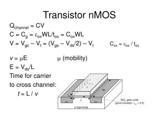
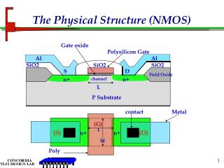
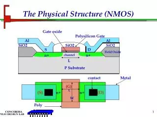
The Physical Structure (NMOS). Gate oxide. Polysilicon Gate. Al. Al. SiO2. SiO2. SiO2. S. D. Field Oxide. Field Oxide. n+. channel. n+. L. P Substrate. contact. Metal. (G). L. (S). (D). n+. n+. W. Poly.

E N D
The Physical Structure (NMOS) Gate oxide Polysilicon Gate Al Al SiO2 SiO2 SiO2 S D Field Oxide Field Oxide n+ channel n+ L P Substrate contact Metal (G) L (S) (D) n+ n+ W Poly
RS Rch RD Transistor Resistance Two Components: Drain/ Sources Resistance: RD(S) = Rsh x no. of squares+ contact resistance. Channel Resistance: Depends on the region of operation: (G) : L (S) (D) n+ n+ W Linear Saturation
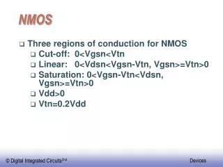
NMOS Operation-Linear KN=K’. W/L Process Transconductance uA/V2 for 0.35u, K’ (Kp)=196uA/ V2 Gate oxide capacitance per unit area eox = 3.9 x eo = 3.45 x 10⁻¹¹ F/m tox Oxide thickness for 0.35 m , tox=100Ao Quick calculation of Cox: Cox= 0.345/tox (Ao) pf/um2 m = mobility of electrons 550 cm2/V-sec for 0.35 m process
NMOS Operation-Linear Effect of W/L Effect of temperature W W Rds W/L temp Rds m
Variations in Width and Length polysilicon 1. Width Oxide encroachment Weff= Wdrawn-2WD 2. Length Lateral diffusion LD= 0.7Xj Leff= Ldrawn-2LD Weff WD WD Wdrawn polysilicon Ldrawn LD Leff LD
Large Transistors • Rchannel decrease with increase of W/L of the transistor
Semiconductor Resistors Resistance R= p(l /A) = (p/t). (l /w) = Rsh. (l /w) Rsh = Sheet resistance / For 0.5u process: N+ diffusion : 70 / M1: 0.06 P+ diffusion : 140 / M2: 0.06 Polysilicon : 12 / M3: 0.03 Polycide:2-3 / P-well: 2.5K N-well: 1K current t l w (A)
Semiconductor Resistors polysilicon Diffusion n+ Al Al SiO2 Field oxide n+ Polysilicon Resistor Diffusion Resistor
Semiconductor Capacitors 1. Poly Capacitor: a. Poly to substrate b. Poly1 to Poly2 2. Diffusion Capacitor sidewall capacitances depletion region n+ (ND) bottomwall capacitance substrate (NA)
Dynamic Behavior of MOS Transistor Prentice Hall/Rabaey
SPICE Parameters for Parasitics Prentice Hall/Rabaey
SPICE Transistors Parameters Prentice Hall/Rabaey
Modelling: Resistance 1. Resistance: Rint= Rsh [l/w] Rsh values for 0.35u CMOS Process: Polysilicon 10 / Polycide 2 / Metal1 0.07 / Metal II 0.07 / Metal III 0.05 / Contact resistance: PolyI to MetalI 50 Via resistance: Metal I to Metal II 1.5 Via resistance: Metal II to metal III 1.
CMOS Inverter: Steady State Response V V DD DD R on V = V OH DD V V = 0 out V OL out R on V = V V = 0 in DD in
Switching Characteristics of Inverters Transient Response
Computing the Capacitances V V DD DD M 2 M 4 C C g 4 db 2 C gd 12 V V V out out 2 in C C C db 1 w g 3 M 3 M 1 Interconnect Fanout V V in out Simplified C Model L
VDD=5V S G VDD MP D Vin Vo D CL G MN S GND Step Response Fall Delay Time: TPHL MN OFF Saturation Linear IDN V = 5 in Vin V = 4 in V = 3 in Vo VDD-VT VDD (VDSAT)
Step Response- Fall time, tf vo 1 0.9 1-n vin tf=~ k is a constant 0.1 td1 td2 0.1 tr=~ k is a constant
Step Response-tPHL Assume normalized voltages vin= Vin/ VDD vo= Vo/ VDD n = VTN/ VDD p = VTP/ VDD tPHL=td1+td2 Vo VDD VDD-VTN Vx VDD/ 2 Vin td1 td2 vo 1 1-n 0.5 vin td1 td2
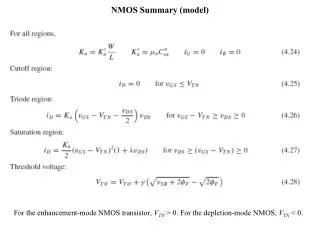
Step Response Rise Delay tPLH and Rise Time tr VDD S G VDD MP D Vin Vo D 0.1 CL G MN S (P= - 0.2) GND
Factors Influence Delay • Inverter Delay,td = (tPHL+tPLH)/2 • The following factors influence the delay of the inverter: • Load Capacitance • Supply Voltage • Transistor Sizes • Junction Temperature • Input Transition Time
Delay as a function of Transistor Size • tPHL and tf decrease with the increase of W/L of the NMOS • tPLH and tr decrease with the increase of W/L of the PMOS
Temperature Effect • Temperature ranges: commercial : 0 to700C industrial: -40 to 850C military: -55 to 1250C • Calculation of the junction temperature tj= ta + ja X Pd • Effect of temperature on mobility • Delay and speed implications
Effect of Input Transition Times The delay of the inverter increases with the increase of the input transition times r and f tPHL = (tPHL) step + (r /6).(1-2p) tPLH = (tPLH) step + (f/6).(1+2n) Vo r Vin
Transistor Sizing • Define = (W/L)p/(W/L)n • For Equal Fall and Rise Delay • KN=KP • = n/ p • For Minimum Delay • dtD/d = 0 • opt = Sqrt (n/ p)
Two Components contribute to the power dissipation: Static Power Dissipation Leakage current Sub-threshold current Dynamic Power Dissipation Short circuit power dissipation Charging and discharging power dissipation Power Dissipation in CMOS
Static Power Dissipation VDD • Leakage Current: • P-N junction reverse biased current: • io= is(eqV/kT-1) • Typical value 0.1nA to 0.5nA @room temp. • Total Power dissipation: • Psl= i0.VDD • Sub-threshold Current • Relatively high in low threshold devices S G B MP D Vin Vo D G B MN S GND
Analysis of CMOS circuit power dissipation • The power dissipation in a CMOS logic gate can be • expressed as • P = Pstatic + Pdynamic • = (VDD · Ileakage) + (p · f · Edynamic) • Where p is the switching probability or activity factor • at the output node (i.e. the average number of output • switching events per clock cycle). • The dynamic energy consumed per output switching event is defined as Edynamic =
Analysis of CMOS circuit power dissipation The first term —— the energy dissipation due to the Charging/discharging of the effective load capacitance CL. The second term —— the energy dissipation due to the input-to-output coupling capacitance. A rising input results in a VDD-VDD transition of the voltage across CM and so doubles the charge of CM. CL = Cload + Cdbp +Cdbn CM = Cgdn + Cgdp
The MOSFET parasitic capacitances • • distributed, • • voltage-dependent, and • • nonlinear. • So their exact modeling is quite complex. Even ESC can be modeled, it is also difficult to calculate the Edynamic. On the other hand, if the short-circuit current iSC can be Modeled, the power-supply current iDD may be modeled with the same method. So there is a possibility to directly model iDD instead of iSC.
Analysis of short-circuit current The short-circuit energy dissipation ESC is due to the rail-to-rail current when both the PMOS and NMOS devices are simultaneously on. ESC = ESC_C + ESC_n Where and
Charging and discharging currents • Discharging Inverter Charging Inverter
Factors that affect the short-circuit current For a long-channel device, assuming that the inverter is symmetrical (n = p = and VTn = -VTp = VT) and with zero load capacitance, and input signal has equal rise and fall times (r = f = ), the average short-circuit current [Veendrick, 1994] is From the above equation, some fundamental factors that affect short-circuit current are: , VDD, VT, and T.
Parameters affecting short cct current For a short-channel device, and VT are no longer constants, but affected by a large number of parameters (i.e. circuit conditions, hspice parameters and process parameters). CL also affects short-circuit current. Imean is a function of the following parameters (tox is process-dependent): CL, , T (or /T), VDD, Wn,p, Ln,p (or Wn,p/Ln,p ), tox, … The above argument is validated by the means of simulation in the case of discharging inverter,