Download
1 / 42
420 likes | 622 Views
ECE 506 Reconfigurable Computing http://www.ece.arizona.edu/~ece506 Lecture 3 Reconfigurable Architectures Ali Akoglu. Complex Programmable Logic Device. Hierarchical design against size explosion of PLAs C ombinational logic with Flip Flops (registered output)

E N D
ECE 506Reconfigurable Computinghttp://www.ece.arizona.edu/~ece506Lecture 3Reconfigurable ArchitecturesAli Akoglu
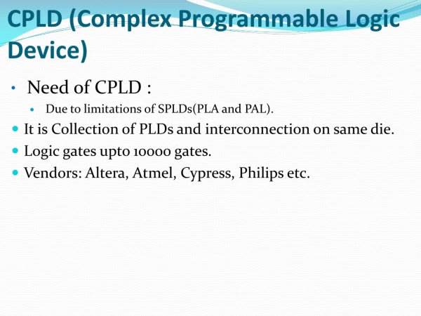
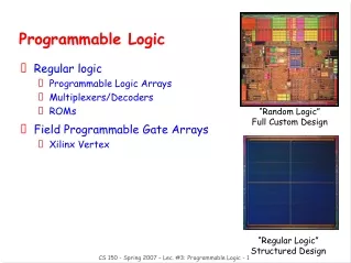
Complex Programmable Logic Device • Hierarchical design against size explosion of PLAs • Combinational logic with Flip Flops (registered output) • Organized into logic blocks connected in an interconnect matrix • Usually enough logic for simple counters, state machines, decoders, etc.
Xilinx CoolRunner II CPLD • PLA and Macrocell combination • 1.8V device, estimated power consumption of less than 100 micro amps • Up to 12,000 gates, 512 MacroCells
CPLD • Multiple Function Blocks (FBs) and I/O Blocks (IOBs) • Fully interconnected (FB outputs and input signals to the FB Inputs) • Each FB provides programmable logic 54 inputs,18 outputs. • The IOB provides buffering for device inputs and outputs. • Output enable signals drive directly to the IOBs.
Function Block • Comprised of 18 independent macrocells, • Each can implement a combinatorial or registered function. • Logic within the FB is implemented using a sum-of-products representation. • Fifty-four inputs (108 true and complement signals) into the programmable AND-array to form 90 product terms. • Any number of these product terms, can be allocated to each macrocell by the product term allocator. How many product terms would you assign for each Macrocell?
Macrocell configured for a combinatorial or registered function. Product Term Allocator selects: 5 product terms primary data inputs to the OR gate for combinatorial functions, as control inputs (clock, clock enable, set, reset, output en.)
Product Term Allocator • Controls how the five direct product terms are assigned to each MC. • For example, all five direct terms can drive the OR function .
Product Term Allocator • Can re-assign other product terms within the FB to increase the logic capacity of a macrocell beyond five direct terms. • Any macrocellrequiring additional product terms can access uncommitted product terms in other macrocells within the FB. • Up to 15 product terms can be available to a single macrocell with only a small incremental delay (tPTA)
Product Term Allocator • Can re-assign product terms from any macrocell within the FB by combining partial sums of products over several macrocells • What is the incremental delay in this example 2tPTA If all 90 product terms are available to any macrocell, what is the maximum incremental delay?
Programmability Options • PLDs, CPLDs have different types of programmability. • initial programming and reprogramming • One-time programmable: • device is programmed once and holds its programming "forever" • usually uses fuses to make/break links • not reusable, but usually the cheapest • discard device if changes are to be made
Programmability Options • UV-Erasable (EPROM) • a floating gate positioned between regular MOS transistor control gate and the channel. • floating gate is uncharged • To program the cell: • a high voltage (e.g. 14 volts) applied to the control gate (drain is at ~12 volts). • causes current to flow between the source and drain. • accelerates electrons to high velocity and a small fraction of them traverse the thin oxide and become trapped on the floating gate. • floating gate, surrounded by an insulating layer, becomes “permanently” negatively charged and the transistor is permanently turned off. • “Permanent” means about 10 years at 125 degrees C; at higher temperatures this time is reduced. • Cells erased by Ultra-Violet (UV) light. • electrons on floating gates are excited and discharged to the substrate.
Programmability Options • Electrically Erasable (EEPROM) • uses a floating gate structure with a control gate on top. • both erasing and reprogramming is accomplished with an electrical current • device can be programmed/erased on circuit board, no special packaging or IC socket is needed • erase time is much faster than UV erase • programming retained after power down • non-volatile • programming/erasing limited to 1000s of cycles
Programmability Options • Electrically Erasable: • both erasing and reprogramming is accomplished with an electrical current • device can be programmed/erased on circuit board, no special packaging or IC socket is needed • erase time is much faster than UV erase • programming retained after power down • non-volatile • programming/erasing limited to 1000s of cycles
Electrically Erasable PLDs • Conventional PLDs are either • One-time programmable • UV Erasable • Must be placed in a programmer to program them • EE PLDs can be programmed and erased in place • A small (four wire) connection to a computer is needed • Once programmed, will retain program indefinitely • Never have to take the chip out of its circuit
FPGA • Introduced in 1985 by Xilinx • Similar to CPLDs • A function to be implemented in FPGA • Partitioned into modules , each implemented in a logic block. • Logic blocks connected with the programmable interconnection.
FPGA Technology • 1) Antifuse-based • Realization of interconnections • 2) Memory-based. • realization of interconnections and computation • FLASH, SRAM
FPGA Technology • Antifuse FPGAs: • configured by burning a set of fuses. • once configured, cannot be altered any more • bug fixes and updates possible for new PCBs, but hardly for already manufactured boards. • ASIC replacement for small volumes. • Flash FPGAs • may be re-programmed several thousand times and are non-volatile • Expensive, re-configuration takes several seconds • SRAM FPGAs • dominating technology • unlimited re-programming • additional circuitry is required to load the configuration into the FPGA after power on • re-configuration is very fast, • Some devices allow even partial re-configuration during operation
Antifuse (Actel FPGA) • An antifuse is normally an open circuit. • Two-terminal elements connected to upper and lower layer of the antifuse, in the middle is a dielectric (Oxygen-Nitrogen-Oxygen, ONO) layer • Initial state: • High resistance of dielectric does not allow any current to flow. • Applying a high voltage: • causes large power dissipation and melts the dielectric • Drastically reduces the resistance • a link can be built, which permanently connects the two layers.
Antifuse chips • Advantage ! • Small area • With metal-to-metal anti-fuses, no silicon area is required to make connections, decreasing the area overhead of programmability. • Much lower resistance and parasitic capacitance over transistors. • possible to include more switches per device • reduces the RC delays in the routing. • No bitstream can be intercepted in the field (no bitstreamtransfer) • Need a Scanning Electron Microscope to try to know antifusestates (an Actel AX2OOO antifuse FPGA contains 53 million antifuses with only 2-5% programmed in an average design) • Interconnect structure is naturally “rad hard,” • relatively immune to the effects of radiation (except flip-flops!), • SRAM-based component can be “flipped” if hit by radiation
Antifuse chips • Disadvantage ! • not suitable for devices that must be frequently reprogrammed • one-time programmable FPGAs. • special programmers must be used to program a device before it is mounted on a final product • involves significant changes to the properties of the materials in the fuse, • leads to scaling challenges when new IC fabrication processes are considered
Programmability Options • Static Random Access Memory (SRAM) Programming: • Switch is a pass transistor controlled by the state of the SRAM bit • Logic block configuration bits are stored in SRAM • can be reprogrammed infinite number of times • use of standard CMOS process technology • SRAM cells are created using exactly the same CMOS technologies as the rest of the device, • No special processing steps are required in order to create these components. • benefit from the increased integration, higher speeds and lower dynamic power consumption of new processes with smaller minimum geometries.
Programmability Options • SRAM Volatility • programming contents NOT retained after power down • external non-volatile memory device required on power up • SRAM Size • SRAM cell requires either 5 or 6 transistors and the programmable element used to interconnect signals requires at least a single transistor. • SRAM Security • Since the configuration information must be loaded into the device at power up, there is the possibility that the configuration information could be intercepted and stolen for use in a competing system.
Programmability Options • Flash Programming: • alternative that addresses some of the shortcomings of SRAM • Use of floating gate programming technologies • inject charge onto a gate that “floats” above the transistor. • Non-volatile • eliminates the need for the external storage for configuration data • can function immediately upon power-up • Area efficiency • Area overhead: The programming circuitry (high and low voltage buffers) needed to program the cell, • Cost is relatively modest as it is amortized across numerous programmable elements.
Programmability Options • Cannot be reprogrammed an infinite number of times. • Charge buildup in the oxide eventually prevents a flash-based device from being properly erased and programmed • Non-standard CMOS process. • around five additional process steps on top of standard CMOS • behind SRAM-based devices by one or more generations. • Programming time is about three times that of an SRAM-based component. • High resistance and capacitance due to the use of transistor-based switches. • Solution: on-chip flash memory to provide non-volatile storage with SRAM cells to control the programmable elements in the design.
Programmability Options • An ideal technology • non-volatile • reprogrammable • using a standard CMOS process • offer low on resistances and low parasitic capacitances.
FPGA Components • How can we implement any circuit in an FPGA? • Example: Half adder • Combinational logic represented by truth table • What kind of hardware can implement a truth table?
FPGA Components • Lookup Table (LUT) • Implement truth table in small memories (LUTs) • Usually SRAM • A function is implemented by writing all possible values that the function can take in the LUT • The inputs values are used to address the LUT and retrieve the value of the function corresponding to the input values 2-input, 1-output LUTs 00 00 Addr Addr A 01 A 01 10 B B 10 11 11 Output Output C S
FPGA Components • Alternatively, could have used a 2-input, 2-output LUT • Outputs commonly use same inputs 00 00 00 Addr Addr Addr A 01 A A 01 01 B 10 10 10 B B 11 11 11 S C C S
FPGA Components • Slightly bigger example: Full adder • Combinational logic can be implemented in a LUT with same number of inputs and outputs • 3-input, 2-ouput LUT 3-input, 2-output LUT Truth Table A B Cin S Cout
FPGA Components • LUT Example: Implement the function ABD+BCD+ABC • 2-input LUTs • 3-input LUTs • 4-input LUTs
FPGA Components • LUTs are used as function generators • How many SRAM locations does a k-input LUT have? • How many different functions can a k-input LUT implement? 2k 22k 00 Addr A 01 B 10 11 C S
FPGA Components • Why aren’t FPGAs just a big LUT? • Size of truth table • grows exponentially based on # of inputs • 3 inputs = 8 rows, 4 inputs = 16 rows, 5 inputs = 32 rows, etc. • Same number of rows in truth table and LUT • LUTs grow exponentially based on # of inputs • Number of SRAM bits in a LUT • = 2i * o • i = # of inputs, o = # of outputs • Example: 64 input combinational logic with 1 output would require 264 SRAM bits • 1.84 x 10¹⁹ • Clearly, not feasible to use large LUTs • So, how do FPGAs implement logic with many inputs?
FPGA Components • Fortunately, we can map circuits onto multiple LUTs • Divide circuit into smaller circuits that fit in LUTs (same # of inputs and outputs) • Example: 3-input, 2-output LUTs
FPGA Components • Large LUTs • Fast when using all inputs • Wastes transistors otherwise • Must also consider total chip area • Wasting transistors may be ok if there are plenty of LUTs
FPGA Components • What if circuit doesn’t map perfectly? • More inputs in LUT than in circuit • Truth table handles this problem • More outputs in LUT than in circuit • Extra outputs simply not used • Space is wasted, so should use multiple outputs whenever possible • Important Point • The number of gates in a circuit has no effect on the mapping into a LUT • All that matters is the number of inputs and outputs • Unfortunately, it isn’t common to see large circuits with a few inputs 1,000,000 gates 1 gate
FPGA Components • LUT-Realization • A LUT is basically a multiplexer that evaluates the truth table stored in the configuration SRAM cells (can be seen as a one bit wide ROM).
FPGA Components • Example: • Determine best LUTs for following circuit • Choices • 4-input, 2-output LUT (delay = 2 ns) • 6-input, 2-output LUT (delay = 3 ns) • Assume each SRAM cell is 6 transistors • 4-input LUT = 6 * 24 * 2 = 192 transistors • 6-input LUT = 6 * 26 * 2 = 384 transistors
FPGA Components • Example: • Determine best LUTs for following circuit • Choices • 4-input, 2-output LUT (delay = 2 ns) • 6-input, 2-output LUT (delay = 3 ns) • Assume each SRAM cell is 6 transistors • 4-input LUT = 6 * 24 * 2 = 192 transistors • 6-input LUT = 6 * 26 * 2 = 384 transistors 6-input LUT Propagation delay = 3 ns Total transistors = 384
FPGA Components • Example: • Determine best LUTs for following circuit • Choices • 4-input, 2-output LUT (delay = 2 ns) • 6-input, 2-output LUT (delay = 3 ns) • Assume each SRAM cell is 6 transistors • 4-input LUT = 6 * 24 * 2 = 192 transistors • 6-input LUT = 6 * 26 * 2 = 384 transistors 4-input LUT Propagation delay = 4 ns Total transistors = 384 transistors 6-input LUTs are 1.3x faster and use same area
FPGA Components • Problem: How to handle sequential logic • Truth tables don’t work • Possible solution: • Add a flip-flop to the output of LUT • BLEs: the basic logic element • Circuit can now use output from LUT or from FF • Where does select come from?