Download
1 / 91
910 likes | 971 Views
Explore the design and analysis of sequential circuits featuring state diagrams, tables, state assignments, and logic expressions. Learn about clock cycles, flip-flops, combinational circuits, and implementations in Verilog code.

E N D
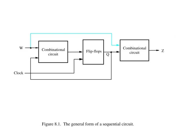
W Combinational Combinational Z Flip-flops circuit circuit Q Clock Figure 8.1. The general form of a sequential circuit.
Clockcycle: t t t t t t t t t t t 0 1 2 3 4 5 6 7 8 9 10 w : 0 1 0 1 1 0 1 1 1 0 1 z : 0 0 0 0 0 1 0 0 1 1 0 Figure 8.2. Sequences of input and output signals.
Reset w = 1 ¤ ¤ A z = 0 B z = 0 w = 0 w = 0 w = 1 w = 0 ¤ C z = 1 w = 1 Figure 8.3. State diagram of a simple sequential circuit.
Next state Present Output z state w = 0 w = 1 A A B 0 B A C 0 C A C 1 Figure 8.4. State table.
Y y 1 1 w Combinational Combinational z circuit circuit Y y 2 2 Clock Figure 8.5. A general sequential circuit.
Next state Present Output w = 0 w = 1 state z y y Y Y Y Y 2 1 2 1 2 1 00 00 01 A 0 01 00 10 B 0 10 00 10 C 1 11 dd dd d Figure 8.6. A state-assigned table.
y y 2 1 Ignoring don't cares Using don't cares 00 01 11 10 w 0 0 0 d 0 Y = wy y Y = wy y 1 2 1 2 1 1 1 1 0 d 0 y y 2 1 w 00 01 11 10 0 0 0 d 0 Y = wy y + wy y Y = wy + wy 2 1 2 1 2 2 1 2 1 0 1 d 1 ( ) = w y + y 1 2 y 1 y 2 0 1 0 0 0 z = y y z = y 1 2 2 1 1 d Figure 8.7. Derivation of logic expressions.
t t t t t t t t t t t 0 1 2 3 4 5 6 7 8 9 10 1 Clock 0 1 w 0 1 y 1 0 1 y 2 0 1 z 0 Figure 8.9. Timing diagram.
R 1 out R 1 in w R 2 out Control R 2 circuit in R 3 out Clock R 3 in Done Figure 8.10. Signals needed in Example 8.1.
w = 0 ¤ A No Reset transfer w = 1 ¤ , B R 2 = 1 R 3 = 1 out in w = 0 w = 1 w = 0 w = 1 ¤ , C R 1 = 1 R 2 = 1 out in w = 0 w = 1 ¤ , , D R 3 = 1 R 1 = 1 Done = 1 out in Figure 8.11. State diagram.
Next state Outputs Present state w = 0 w = 1 A A B 0 0 0 0 0 0 0 B C C 0 0 1 0 0 1 0 C D D 1 0 0 1 0 0 0 D A A 0 1 0 0 1 0 1 Figure 8.12. State table.
Next state Present Output state w = 0 w = 1 z y y Y Y Y Y 2 1 2 1 2 1 A 00 00 01 0 B 01 00 11 0 C 11 00 11 1 10 dd dd d Figure 8.16. Improved state assignment for the sequential circuit in Figure 8.4.
Y y 2 2 z Q D Q Y y 1 1 w Q D Q Clock Resetn Figure 8.17. Final circuit for the improved state assignment.
Figure 8.18. Improved state assignment for the sequential circuit in Figure 8.12.
y y 2 1 w 00 01 11 10 0 1 Y = wy + y y 2 2 1 1 1 1 1 y y 2 1 w 00 01 11 10 0 1 1 Y = y 2 1 1 1 1 Figure 8.19. Derivation of next-state expressions.
Nextstate Present Output state w = 0 w = 1 z y y y Y Y Y Y Y Y 3 2 1 3 2 1 3 2 1 A 001 001 010 0 B 010 001 100 0 C 100 001 100 1 Figure 8.20. One-hot state assignment for the sequential circuit in Figure 8.4.
Figure 8.21. One-hot state assignment for the sequential circuit in Figure 8.12.
Clock cycle: t t t t t t t t t t t 0 1 2 3 4 5 6 7 8 9 10 w : 0 1 0 1 1 0 1 1 1 0 1 z : 0 0 0 0 1 0 0 1 1 0 0 Figure 8.22. Sequences of input and output signals.
Reset ¤ w = 1 z = 0 ¤ ¤ w = 0 z = 0 w = 1 z = 1 A B ¤ w = 0 z = 0 Figure 8.23. State diagram.
z Next state Output Present state w = 0 w = 1 w = 0 w = 1 A A B 0 0 B A B 0 1 Figure 8.24. State table.
Next state Output Present state w = 0 w = 1 w = 0 w = 1 y Y Y z z A 0 0 1 0 0 B 1 0 1 0 1 Figure 8.25. State-assigned table.
z w Q D y Clock Q Resetn (a) Circuit t t t t t t t t t t t 0 1 2 3 4 5 6 7 8 9 10 1 Clock 0 1 w 0 1 y 0 1 z 0 (b) Timing diagram Figure 8.26. Implementation of FSM in Figure 8.25.
Figure 8.27. Circuit that implements the specification in Figure 8.2.
w = 0 Reset A ¤ , w R R = 1 2 = 1 3 = 1 out in B w = 0 , R R 1 = 1 2 = 1 out in w = 1 C w = 0 , , R R Done 3 = 1 1 = 1 = 1 out in w = 1 Figure 8.28. State diagram for Example 8.4.
module simple (Clock, Resetn, w, z); input Clock, Resetn, w; output z; reg [2:1] y, Y; parameter [2:1] A = 2'b00, B = 2'b01, C = 2'b10; // Define the next state combinational circuit always @(w or y) case (y) A: if (w) Y = B; else Y = A; B: if (w) Y = C; else Y = A; C: if (w) Y = C; else Y = A; default: Y = 2'bxx; endcase // Define the sequential block always @(negedge Resetn or posedge Clock) if (Resetn == 0) y <= A; else y <= Y; // Define output assign z = (y == C); endmodule Figure 8.29. Verilog code for the FSM in Figure 8.3.
Please see “portrait orientation” PowerPoint file for Chapter 8 Figure 8.30. Implementation of an FSM in a CPLD.
module simple (Clock, Resetn, w, z); input Clock, Resetn, w; output z; reg z; reg [2:1] y, Y; parameter [2:1] A = 2'b00, B = 2'b01, C = 2'b10; // Define the next state combinational circuit always @(w or y) begin case (y) A: if (w) Y = B; else Y = A; B: if (w) Y = C; else Y = A; C: if (w) Y = C; else Y = A; default: Y = 2'bxx; endcase z = (y == C); //Define output end // Define the sequential block always @(negedge Resetn or posedge Clock) if (Resetn == 0) y <= A; else y <= Y; endmodule Figure 8.33. Second version of code for the FSM in Figure 8.3.
module simple (Clock, Resetn, w, z); input Clock, Resetn, w; output z; reg [2:1] y; parameter [2:1] A = 2'b00, B = 2'b01, C = 2'b10; // Define the sequential block always @(negedge Resetn or posedge Clock) if (Resetn == 0) y <= A; else case (y) A: if (w) y <= B; else y <= A; B: if (w) y <= C; else y <= A; C: if (w) y <= C; else y <= A; default: y <= 2'bxx; endcase // Define output assign z = (y == C); endmodule Figure 8.34. Third version of code for the FSM in Figure 8.3.
Please see “portrait orientation” PowerPoint file for Chapter 8 Figure 8.35. Verilog code for the FSM in Figure 8.11.
Please see “portrait orientation” PowerPoint file for Chapter 8 Figure 8.36. Verilog code for the Mealy machine of Figure 8.23.
Figure 8.38. Potential problem with asynchronous inputs to a Mealy FSM.
A a Shift register s Adder Shift register FSM Shift register b Sum A B = + B Clock Figure 8.39. Block diagram of a serial adder.
s Next state Output Present state ab =00 01 10 11 00 01 10 11 G G G G H 0 1 1 0 H G H H H 1 0 0 1 Figure 8.41. State table for the serial adder.
Next state Output Present state ab =00 01 10 11 00 01 10 11 y Y s 0 0 0 0 1 0 1 1 0 1 0 1 1 1 1 0 0 1 Figure 8.42. State-assigned table for the serial adder.
s a Full b adder Y y Q D carry-out Clock Q Reset Figure 8.43. Circuit for the adder FSM.
Reset 11 01 ¤ ¤ G s = 0 H s = 0 00 0 0 10 00 01 01 00 11 11 10 10 01 ¤ ¤ G s = 1 H s = 1 11 1 1 10 00 Figure 8.44. State diagram for the Moore-type serial adder FSM.
Nextstate Present Output state ab =00 01 10 11 s G G G G H 0 0 0 1 1 0 G G G G H 1 1 0 1 1 0 H G H H H 0 0 1 0 0 1 H G H H H 1 1 1 0 0 1 Figure 8.45. State table for the Moore-type serial adder FSM.
Nextstate Present Output ab state =00 01 10 11 y y s 2 1 Y Y 2 1 00 0 0 01 0 1 10 0 01 0 0 01 0 1 10 1 10 0 1 10 1 0 11 0 11 0 1 10 1 0 11 1 Figure 8.46. State-assigned table for the Moore-type serial adder FSM.
y Y Sum bit 1 1 a s Q D Full b adder Carry-out Q Y y 2 2 Q D Clock Q Reset Figure 8.47. Circuit for the Moore-type serial adder FSM.
module shiftrne (R, L, E, w, Clock, Q); parameter n = 8; input [n-1:0] R; input L, E, w, Clock; output [n-1:0] Q; reg [n-1:0] Q; integer k; always @(posedge Clock) if (L) Q <= R; else if (E) begin for (k = n-1; k > 0; k = k-1) Q[k-1] <= Q[k]; Q[n-1] <= w; end endmodule Figure 8.48. Code for a left-to-right shift register with an enable input.
Please see “portrait orientation” PowerPoint file for Chapter 8 Figure 8.49. Verilog code for the serial adder.
1 0 0 0 a a D D D D 7 0 3 2 1 0 L Counter E L w 0 Q Q Q Q 3 2 1 0 1 E Adder b b FSM 7 0 Run L 0 0 w 0 1 E L w E Clock Reset Sum Sum 7 0 Figure 8.50a. Synthesized serial adder.