Sequential Circuit Design
Sequential Circuit Design. Shmuel Wimer Bar Ilan University, Engineering Faculty Technion, EE Faculty. clock. clock. clock. data. Q. data. Q. Latch. Flop. Q-latch. Q-flop. Latch is transparent on high clock and opaque on low clock.

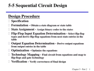
Sequential Circuit Design
E N D
Presentation Transcript
Sequential Circuit Design Shmuel Wimer Bar Ilan University, Engineering Faculty Technion, EE Faculty
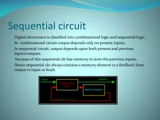
clock clock clock data Q data Q Latch Flop Q-latch Q-flop Latch is transparent on high clock and opaque on low clock. Flip-flop is edge triggered. It transfers input data to Q on clock rising edge. Memory Elements data
clk clk TC Flop Flop Combinational Logic Static Sequencing by Flip-Flops One flip-flop is used on each cycle boundary. Tokens advance from one cycle to the next on rising edge.
TC tnonoverlap Φ1 TC/2 tnonoverlap Φ2 Φ1 Φ1 Φ2 Latch Latch Latch Combinational Logic Combinational Logic Half-Cycle 1 Half-Cycle 2 Static Sequencing by Latches 2-phase system. Phases may be separated by some non overlapping time.
TC tpw Φp Φp Latch Latch Combinational Logic Static Sequencing by Pulsed Latches
Latch Latch Latch Latch Combinational Logic Flip-Flop Flip-Flop Flip-flop sequencing can be viewed as a back-to-back latch pair
A Y clk clk Flop D Q D Q Combinational Logic A Y
D clk clk Latch Q D Latch is transparent when clock is high. In order for a data change to transfer to output, the latest change must occur at tsetup before latch turns to opaque. It must sustain thold after latch turns opaque.
D Q clk clk Latch Q D When a latch turns transparent the data is transferred to output at min delay of tccqand max delay of tpcq. Data change at transparency is transferred to output at min delay of tcdq and max delay of tpdq.
clk clk D2 Q1 TC Combinational Logic FF1 FF2 clk Q1 D2 Max-Delay Constraints
Φ1 Φ1 Φ2 Φ2 Φ1 D1 D2 D3 Q1 Q2 Q3 D1 L1 L3 L2 Combinational Logic Combinational Logic Q1 D2 Q2 D3 TC
Notice that the non overlap between clocks doesn’t degrade performance. Flip-Flop can be realized by two latches connected back to back, yielding expression similar to Flip-Flop sequencing.
Q1 Q2 D1 D2 tpw TC D2 Φp Φp D1 L1 L2 Combinational Logic Q1
If the pulse width is wide enough the max delay is similar to two-phase latches, except that only one latch is in the critical path. If the pulse width is narrower than the setup time, the data must be set up before the pulse falls.
Q1 Q2 D1 D2 TC Q1 Φp Φp D2 L1 L2 Combinational Logic tpw Consequently:
Min-Delay Constraints Logic circuits cannot be too fast. Otherwise the input data to next sequential circuit will change while it is still holding its current data. Such malfunction is called race condition, hold time failure or min-delay failure.
clk clk D2 Q1 Combinational Logic FF1 FF2 clk Q1 D2
Φ2 D1 D2 Q1 Q2 L1 tnonoverlap Φ1 L2 Combinational Logic Φ2 Q1 D2 Φ1
Taking large enough non overlapping time will avoid min delay problems, but distributing two clocks and controlling non overlapping time is difficult and expensive. Latch-based systems are usually using single clock and its complement, making non overlapping time be zero. In that case min delay constraint for flip-flop and latches is the same.
Here is a paradox: The logic in latch-based system requires twice min-delay as in flip-flop. On the other hand flip-flop can be built by a pair of latches! The resolution follows from the fact that a flip-flop has an internal race condition, making its hold time longer than in latch.
Φp D1 D2 Q1 Q2 L1 L2 Combinational Logic tpw Q1 Φp D2
Time Borrowing In flip-flop systems clock sharply delineates the cycles. Hence clock imposes hard edge. Latch systems are more flexible due to latch transparency. Data input of a latch must set up before falling edge.
Φ1 Φ1 Φ2 Φ1 Φ2 Latch Borrowing time across half-cycle boundary Borrowing time across pipeline stage boundary Latch Latch Combinational Logic Combinational Logic
Φ1 Φ2 Φ1 Φ2 Latch Latch Loops may borrow time internally but must complete within the cycle. CL CL
Φ1 Combinational Logic Φ1 Φ2 TC Φ2 D1 D2 Q1 Q2 L1 TC/2 D2 L2
Clock Skew • Clock should theoretically arrive simultaneously to all sequential circuits. • Practically it arrives in different times. The differences are called clock skews. • Clock skew consists of the following components: • Systematic is the portion existing under nominal conditions. It can be minimized by appropriate design. • Random is caused by process variations like devices’ channel length, oxide thickness, threshold voltage, wire thickness, width and space. It can be measured on silicon and adjusted by delay components.
clk clk D2 Q1 TC Combinational Logic FF1 FF2 clk Q1 D2
clk clk D2 Q1 FF1 FF2 Combinational Logic clk Q1 D2 Clock skew worsen max and min delay constraints. Max delay constraint becomes shorter. Min delay constraint becomes longer.
In transparent latch system max delay constraints are not hooked to clock edge since it is assumed that transparency period is long enough. Hence clock skew doesn’t affect max delay constrained. Min delay constraints are worsen however since they depend on the non overlap time, which may effectively be shortened by skew.
Max delay constraint in pulsed latch is not affected if pulse is wide enough. Min delay constrained in pulsed latch is increased since skew effectively increases hold time. It is also reducing time borrowing.
Latches and Flip-flops Buffered output inverting latch Buffered input inverting latch. It is a tristate inverter. Both are fast dynamic latches.
In high leakage, the dynamic latches retain their output value only for a short period and in order to sustain it, latches must be staticized to avoid floating output. Tristate feedback inverter sustains output voltage when clock is low (latch is opaque). Input was also isolated. A noise spike at output may invert the latch output.
f This is a robust non inverting latch addressing all deficiencies To reduced clock load and save two transistors, the tristate can be replaced by a weak inverter, called jamb latch.
Dynamic inverting flip-flop can be constructed by a pair of back-to-back dynamic latches. To reduce delay at the expense of noise sensitivity, either first or last inverters can be removed.
Static non inverting flip-flop is constructed from two static latches.
If clock signal rise / fall time is very slow, it may happen that both latches will be simultaneously transparent, which will require to increase hold time. This can be solved by buffering the clock signal locally at flip-flop, thus sharpening its edges in the expense of more area and clock load.
Another solution is to use nonoverlapping clocks. Making nonoverlapping large enough, large skew can be tolerated. Large nonoverlapping causes however large setup time (sequencing overhead).
Pulsed latch is built from conventional latch driven by a brief clock pulse. The latter is generated by a circuit called clock chopper.
Synchronous resettable latch f Sequencing elements require a reset signal to enter a known initial state or startup. Asynchronous reset forces Q immediately, while synchronous reset waits for clock edge. Reset must be stable for setup and hold time around clock edge.
f f Synchronous resettable flip-flop Reset affects Q only at clock rising
SET f f Asynchronous settable and resettable flip-flop Set and reset must enter in both master and slave stages
D 1 Q FF 0 en Enabling latches and flip-flops Enabling is done on data change. It doesn’t affect clock, but affects delay, adds area and power.
en FF Q D Clock gating doesn’t affect delay but may add clock skew. It significantly reduces power consumption since clock is not toggling on disabled element. AND gate is added to clock driver.
Static Sequencing Methodology • Flip-flops: Most popular in non aggressive deigns. • Simple and robust. • Setup and hold times are penalties. • No time borrowing within clock cycle (unless clock is shifted). • Pulsed Latches: Similar behavior to flip-flops. • Simpler than FF or transparent latches, less area and power. • Faster than FF. • Higher effective hold time, min-delay constraints more difficult.
Transparent Latches: Use in high-end designs • Lower sequencing overhead, faster than FF. • Allows nearly half cycle time borrowing. • Complex clock design, sensitive to clock slew rate
Metastability in a latch At transparency sample switch is closed and hold switch is open. When latch is opaque sample switch is open and hold switch is closed, and the two inverters are connected in a feedback loop.
stable metastable stable Latch can enter into metastable state where voltages are consistent. It can remain so unbounded time!