Download
1 / 15
180 likes | 489 Views
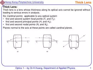
Thick-Film Hybrid Circuitry. Nanotechnology UEET103. Applications of Thick-Film processing. Sensors. High Temperature circuit boards. Displays. Technology. Screen Printing Viscometry Drying and Firing Thickness measurement Electrical Measurement Resistor trim. Screen Printing.

E N D
Thick-Film Hybrid Circuitry Nanotechnology UEET103
Applications of Thick-Film processing Sensors. High Temperature circuit boards. Displays
Technology Screen Printing Viscometry Drying and Firing Thickness measurement Electrical Measurement Resistor trim
Screen Printing Presco 435 Screen-Printer 1 mil alignment accuracy
Viscometry Viscometer used to check the viscosity of a fluid or paste. Stabinger viscometer Rheometer Tank Viscometer
Drying FurnaceFiring Furnace Drying furnaces are used to dry the paste prior to firing. The thickness should be measured after drying. Firing furnace sinters (fuses) particles together. Belt speed and heater temperature sets the profile.
Thickness measurement Profilometer – uses a stylus to trace the thickness profile of a printed line.
Electrical measurements. Various methods are used to measure resistance and capacitance. LCR bridge will measure the impedance where a DC source monitor unit will measure the resistance.
Resistor Trim Uses an infra-red laser to trim through a printed resistor – x,y trim stage.
Materials Depends on mass transport and sintering to fuse into a contiguous film. Conductors and insulators are both available. Semiconductors can also be used. Alumina ceramic is commonly used as a substrate.
Examples. http://www.heraeus-thickfilm.com/media/webmedia_local/media/datasheets/hybridpastes/Schematic_Hybrid_Pb_free_and_plating.pdf
Sintering • Materials Research • Print version ISSN 1516-1439 • Mat. Res. vol.10 no.1 São Carlos Jan./Mar. 2007 • doi: 10.1590/S1516-14392007000100011 • Characterization of ceramic powders used in the inCeram systems to fixed dental Prosthesis
Lawrence Livermore National Laboratory7000 East Avenue, Livermore, CA 94550-9234S&TR Office: (925) 423-3432 Operated by the University of California for the U.S. Department of Energy This image taken with a scanning electron microscope shows the three-dimensional grain structure of a Livermore transparent yttrium–aluminum–garnet ceramic sample.
Metal Sintering Fig. 81: 2D reconstructions (virtual slices) perpendicular to the cylindrical axis showing Cu particles at different stages of the sintering process: (a) before sintering, (b) after sintering at 1000°C, and (c) after sintering at 1050°C. Identical regions (inside the rectangle of (a)) are shown at a higher magnification below Principal Publication and AuthorsO. Lame (a), D. Bellet (a), M. Di Michiel (b) and D. Bouvard (a), European Materials Research Society 2002 Proceedings, to be published in Nuclear Instruments and Methods in Physics Research B.
http://www.ferro.com/non-cms/ems/EPM/LTCC/DESIGN/Paper-3.pdf http://www.thickfilmsolutions.com/pageL1.htm