Download
1 / 31
320 likes | 583 Views
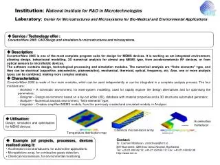
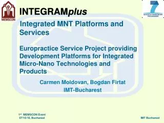
INTEGRAM plus Integrated MNT Platforms and Services Europractice Service Project providing Development Platforms for Integrated Micro- Nano Technologies and Products. Carmen Moldovan, Bogdan Firtat IMT-Bucharest. Laboratory of Microsystems for Environmental and Biomedical Applications.

E N D
INTEGRAMplusIntegrated MNT Platforms and ServicesEuropractice Service Project providing Development Platforms for Integrated Micro-Nano Technologies and Products Carmen Moldovan, Bogdan Firtat IMT-Bucharest IMT Bucharest
Laboratory of Microsystems for Environmental and Biomedical Applications Carmen Moldovan – Head of Laboratory for Environmental and Biomedical Applications –15 years of experience in MEMS technologies • Associate professor • Coordinator and partners of more of 25 national projects and 10 EU projects • Former NEXUS Steering Committee member • ISTAG group member within DG - INFSO, EC Bogdan Firtat – Scientific Researcher, 10 years experience in MEMS technologies: design, simulation and modelling for mechanical, chemical and biological microsensors and FEM microfluidic modelling.
INTEGRAMplus - FP6 Integrated Project Europractice Service Project providing Development Platforms for Integrated Micro-Nano Technologies and Products Carmen Moldovan, IMT Bucharest
Aim: Highly integrated microsystems combining smart Si functionality with polymer platforms in a multi-domain environment Address and stimulate future market needs via higher levels of integration in stable, manufacturable MNT processes enabling nano via micro Emerging markets: biomedical & healthcare; pollution & security; comms (RF & optical) Multi-domain integration: bio-optical-fluidics, MEMS and/or electronics; mixed process technologies (silicon-polymer) Stimulate take up of smart (integrated) MNT products Reduce barriers to MNT access training and standardisation provide development platforms and standard modules Provide low cost MNT prototyping services enable virtual manufacturing based on Design for Manufacture principles Silicon MEMS and polymer prototyping Provide seamless service across the MNT supply chain from concept to production 10 partners from 7 countries + extended supply chain network INTEGRAMplus - Integrated MNT Platforms and Services
PARTNERS Coventor sarl, Paris, France QinetiQ Ltd., Malvern, UK Lancaster University, UK CSEM, Alpnach, Switzerland National Institute for R&D in Microtechnologies, Bucharest, Romania Epigem Ltd., Redcar, UK Institute of Electron Technologies, Warsaw, Poland Institut für Mikrotechnik, Mainz, Germany Yole Dévelopment, Lyon, France Silex, Sweden
INTEGRAMplus Organisation SUPPLY CHAIN PARTNERS Hymite (packaging) X-Fab (CMOS manufacture) AMIS (CMOS manufacture) MCE (packaging) C-MAC (volume assembly) Expert Consultants (PATENT-DfMM members) Micronit (glass manufacture) AML (bonding) DELTA (packaging) CAD TOOLS & VIRTUAL MANUFACTURE IMT (Biointegration & microfluidic design) Coventor (Multi-domain software & Design for Manufacture) ITE (Electronics & microfluidic design) DESIGN SERVICES, PROTOTYPING & LOW VOLUME MANUFACTURE U. Lanc. (PATENT) QinetiQ (silicon) CSEM (polymer, silicon) IMM (polymer) VOLUME MANUFACTURE CUSTOMER SUPPORT Silex Microsystems (Silicon / glass manufacture) EPIGEM (polymer manufacture)
The INTEGRAMplus Partners’ Technology Portfolio European partners in micro and nanotechnologies with complementary expertise in: Silicon, polymer, glass, hybrid solutions Multi-domains (optics, fluidics, MEMS, bio, chemical, electronics) Multi-level integration (material, electronics, functions and system) Development and production along the supply chain FLEXIBLE INTEGRATION Bio-Integration Polymer & Silicon Combined integration Polymer & electrodes DEVICES AND COMPONENTS Microfluidics Micro-Optics Bio-devices Physical sensors Electronics Power sources Memory DSP/µC Comms MATERIALS AND FABRICATION TECHNIQUES Metal deposition Polymer Silicon Glass Bonding Surface Functionalisation Micromachining Moulding Embossing Milling CMOS integration CAPABILITIES FOR WHOLE PRODUCT LIFE CYCLE Design & simulation Prototyping Testing Low and high volume production Packaging Macrosystem integration
INTEGRAMplus offer Products / Production Prototypes Functional Modules Devices & Components Design & Simulation Customers Customers Customers Customers Productisation Fabrication Services Prototyping Services Design Services Consultancy Courtesy IMM Courtesy Epigem Courtesy Epigem Processing
Service Offerings Currently 3 Prototyping Platforms: 1. QinetiQ Silicon MEMS Prototyping Service 2. Epigem Modular Microfluidic Prototyping Service 3. IMM Rapid Prototyping Service for Lab-on-a-chip
Multi-domain Integration - Technological issues Issues being addressed Fabrication of chips with electrodes Competencies needed (Si) chip fabrication Fabrication of polymer parts with electrical leads (injection molding, lithography, … Microchannel fabrication Fabrication of microstructured gaskets (casting, laser cutting, punching, …) Optical components Fabrication of polymer parts (micromachining, casting, embossing, injection molding, …) Surface functionalization Electric contacts between chip and leads (flip-chip, solder bumps, wire bonding, …) Channel sealing Hybrid bonding technologies (surface activation, thermal bonding, …) Microfluidic interfacing Hollow waveguides (fabrication, sealing, integration) Optical interfacing Adhesive bonding technologies (glues, double sided sticky tapes, …) Electrical interfacing Surface functionalization (biochemistry, nanopatterning, …) Connections to macro world (fluid ports & reservoirs, electrical contacts, light contacts) Chip Substrate Underfill Fabrication of silicon/SOI parts (DRIE, anisotropic wet etch, chemical vapour etch, … Integration of silicon into polymer Fluid
INTEGRAMplus multi-domain multi-technology platforms Epigem microfluidics chip with integrated electrodes and pcb headers mounted Hollow waveguide • Advanced optical circuit modules • Combined fluidic and optical modules Si chip scale package with polymer microfluidic chip and electrical connections Innovative silicon-polymer integration technology for chips onto substrates with fluid access opening using flip-chip bonding
INTEGRAMplus Summary Provides industry with a world-leading facility to stimulate take-up and accelerate time-to-market of smart mixed-technology components and solutions. A consortium offering tried and tested micro and nano technology expertise from10 partners operating across 7 European countries. A design and prototyping service with route to volume manufacture for highly integrated microsystems. High degree of flexibility to address the need for increased complexity in microsystems without sacrificing the requirement for manufacturable processes. A flexible customer interactive approach ensures access to INTEGRAMplus at any stage in the product lifecycle. Web-sites: www.integramplus.com www.QinetiQ.com/mems Email: info@integramplus.com Tel: +44(0)1684896262
Mission and main activities • The Laboratory of Microsystems for Biomedical Applications is doing research, focused on development of microsensors and sensors integration such as: • chemosensors (O2, pH, NO2, NOx, CO, CO2, humidity etc.); • biosensors (enzymatic, immunosensors, biomicrosensors array); • nanowire based ISFET • microprobes for recording of electrical activity of cells and tissues, • microfluidic platforms, • signal processing and data acquisition for microsensors array, technologies for sensor integration, data processing, transmission and acquisition. • The Lab is running servicesfor industry in design, simulation, technology, testing and data acquisition, processing and transmission and education in the field of mixed technologies. • The Laboratory was involved in several FP6 projects in the area of technologies for sensors integration, microfluidics and software and hardware development for data acquisition. • IMT’s tasks in the project are: simulation and modelling of fluidics and temperature distribution inside the microsystem channels, and computational modelling of the integrated multi-sensing system. Also IMT will be developing the auxiliary sensors for monitoring the cell culture’s environment and will work on microfluidic microsystem integration. • Resources: The Laboratory has 11 permanent researchers and 2 part time co-workers from a total of 170 employees (researchers and administration).
Sensors technology Gold electrodes pesticide sensor Silicon biochip in the microfluidic module, with pumps and reservoir Conductance and capacitance: A – substrate injection, B – inhibitor injection
NW ISFET sensor Nanowire chip LabView interface Fluid Computer interface Reaction area Enlarged view of the reaction area * Cl. Moldovan, A. Dinescu, E. Manea, R. Iosub, C. Brasoveanu, B. Firtat, C. Moldovan, M. Ion, TECHNOLOGY OF A NANOWIRE BIOFET DEVICE FOR BIOMOLECULES DETECTION , CAS 2009 Proceedings; ISBN: 978-1-4244-4413-7, Vol.2, pag.549-552
Sensors on glass and platform Platform Temperature sensor pH sensor Microfluidic module with the reference electrode
Auxiliary sensor - pH sensor nanofiber polyaniline based SEM picture of electrochemical deposited polyaniline conductive layer in the form of nanofibers Carmen Moldovan, Rodica Iosub, Radu Cornel, Eric Moore, Anna Paschero, Walter Messina, Danilo Demarchi, Cecilia Codreanu, Daniel Necula, Adrian Dinescu, Bogdan Firtat, Sensor system for on-line monitoring of cell cultures, CAS’09 (International Conference on Semiconductors), IEEE catalog Number CFP09CAS-PRT, ISBN: 978-1-424-4412-7; pp 263-267 The pH sensor is a solid state sensor based on conductive polymers, miniaturized, developed on silicon substrate The sensor measurement is a voltage measurement at zero current. The voltage is measured between two electrodes: the active electrode and the reference electrode (Ag/AgCl, KCl 3M). The gold electrode was deposited with a layer of polyaniline conductive emeraldine base form as seen in the SEM. The electrochemical deposited polyaniline has an intrinsic nanowires structure of 100nm diameter
Integration Connections, signal processing, data acquisition, GUI Labview interface Automatic measuring set-up The graphic user interface designed with the LabView. By the program we can control: Acquisition time, Number of loops, Time between the loops, Flow rate in the channels
Integration Microfluidics Visual results of the continuous flow simulation (section through the z plane) – detail The velocity of the fluid into the channel simulation has been performed*** Microfluidic set-up ***B. Firtat, C. Moldovan, G. Boldeiu, FEM Microfluidic simulations for microchannels – continuous and droplet-like flow;The 4M/ICOMM Conference, 23-25 Sept. 2009, Karlsruhe, Germany; Proceedings, pp 205
CO2 GAS SENSORS Electrodes Polysilicon 4000 Å Metal Membrane suporting sensor CVD - SiO2 High dose boron is implanted and diffused followed by a boron doping from solid source + diffusion (1050C, 4 hours). the p-n junction, 12 m depth, for anisotropical stop etch A CVD oxide is deposed such as dielectric layer and the contacts on polysilicon layer are open Cr-Au deposition and configuration follow. Lift-off mask SiO2 5000 Å Si3N4 2000Å Si n <100> B++ Scheme of the sensor chip Si3N4 2000Å
Ceramic gas sensor – integrated heater The input power was 1,1 W and this should be compared with the non-released heater element that requires 2,4 W input power of to reach 490 C The heat distribution from the released heating element using FLIR 40 The power-on curve for the released heater element. The heat distribution of a non- released heater element as seen in figure Non-released heater element
New developments Flexible substrate – gas sensors, batteries
Ink Jet Technology – sensors on paper for gases detection Integration: signal processing, GUI New developments
Design for Manufacture (etch simulations) Calibration of a new software application (Etch3D – developed by Coventor, Inc.), designed for anisotropic silicon etching simulations. • test structures were used, with different sizes and shapes; • the real test structures (etched in both KOH and TMAH, with different temperatures, concentrations and etch times) were compared to the simulation results; • the program’s internal parameters were adjusted, in order to fit the lab results.
Design for Manufacture (etch simulations) SEM picture of the etched test structure (TMAH, 25%, 80º C, 5 min.) Simulation using default values of the program parameters (for TMAH, 25%, 80º C, 5 min.) Tuned values of the program parameters (TMAH, 25%, 80º C, 5 min.). Experimental and simulation results for the 4-crosses test structure (using TMAH)
Microfluidic modelling Microfluidic simulations were performed, in order to analyse one fluid velocity through a specific microchannel design. The simulations were used to observe the flow speed and direction of the liquid passing through, and also dead spots in the flow (zones with much slower velocity), for different fluid flow rates.
Microfluidic modelling • Dead volume and cross contamination • Model compatibility issues solved for different platforms • Several simulations performed: • Continuous flow analysis (velocity, pressure, etc.); • Slug-flow analysis (fluid bubbles through channels); • Identification of fluids cross-contamination and dead-volumes.
Multi-domain modelling • Modelling of a thin membrane silicon pressure sensor • Micro-mechanical simulation (membrane deflection, stress induced); • Electrical and piezoresistive simulation (for determining the current change due to the mechanical stress induced by the applied pressure).
Conclusions Continuing technology development New technologies for platforms develop Offering services: sensors and platform prototyping, simulation, training Interest: New projects partnership Industry attracting, bringing inventions to innovations Start-up development
THANK YOU! carmen.moldovan@imt.ro bogdan.firtat@imt.ro