Download
1 / 20
200 likes | 431 Views
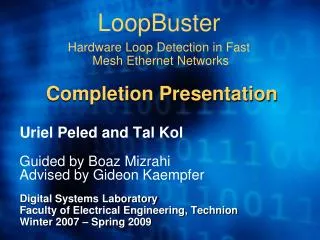
LoopBuster Hardware Loop Detection in Fast Mesh Ethernet Networks. Completion Presentation. Uriel Peled and Tal Kol Guided by Boaz Mizrahi Advised by Gideon Kaempfer Digital Systems Laboratory Faculty of Electrical Engineering, Technion Winter 2007 – Spring 2009.

E N D
LoopBusterHardware Loop Detection in Fast Mesh Ethernet Networks Completion Presentation Uriel Peled and Tal Kol Guided by Boaz Mizrahi Advised by Gideon Kaempfer Digital Systems Laboratory Faculty of Electrical Engineering, Technion Winter 2007 – Spring 2009
LoopBusterStop Loops Without Tree Topology A B Improved Switches: Changed Learning Improved Switches: Changed Learning New Hardware Device: “LoopBuster” Mesh Topology: Loops Allowed! C
Design ChallengesLoopBuster Device • Support very high throughputs • Ethernet supports 1Gbps and 10Gbps links • Implementation must be in hardware • Use limited amount of on-chip memory • Naïve implementation requires 10Mbit for a single 10Gbps interface • Minimal effect on hosting network • Remove looping packets quickly • Minimize false positives • Rely on existing standards / network equipment
Conceptual DiagramLoopBuster Device Filter Filter Filter packet packet packet packet packet packet packet packet packet packet • Still effective – packet rate decreases • We pay with N+1 mandatory loops • Low memory filters in decreasing size
Project Milestones • Full Network Software Simulationpre-hardware implementation • Analyze Algorithm Parameters • Design LoopBuster Device macro, micro architectures, Verilog implementation • Board Bring-up board selection, cores, GbE • Testing, Validation and Debug • Demonstrate Working Prototype
Algorithm ParametersPerformance-Cost Tradeoffs • Number of filter chains • Parallel chains for different MLTTs • Different chains for different traffic types • Number of filters in each chain • Number of loops before terminating a packet • Memory size of each filter in each chain • Minimize false positives while saving memory • Filter scheduling and control patterns • Lock / unlock states, reset filter memory
Algorithm AnalysisEmpirical Param Selection • Network Simulation in Software • Minimal HW (1PC), C++, SW Timeline • Real-world rates, real-world traffic • Based on a genetic algorithm • Genetic representation: filter size list (13,12,10,10,9,9,8,8,7,7,6) • Improve a pre-defined fitness function • False positives over real traffic + Total memory size • Two-stage mutation • General (add/remove filter, change filter size, switch filters) • Specific (num filters, size of largest, create descending chain)
Algorithm AnalysisTheoretical Param Selection • Theoretical algorithm performance analysis • Probability model for a filter / filter chain • C collisions with X packets through an N-bit filter • Occupancy problem, numerical solution in C++
Preliminary Design DecisionAlgorithm Analysis Conclusions • Modular Filter Chain Design • Traffic sensitive • Code / Runtime Configurable Parameters • UART controlled lock/unlock/reset patterns • 2 Clock Domains • 125 MHz (GbE), 31 MHz (Processing) • Packet Pipeline Processing • No store and forward (untraditional MAC) • Hardware only (no Power PC)
Packet Transceiver Block Diagram 125 MHz clock boundary Ethernet data in 8-bit units 31 MHz clock boundary Ethernet data in 32-bit units
LoopBuster FilterImplementation • Supports two concurrent packet paths • Unique clock domain: 125 MHz • lb_filter_memory (Memory) • Filter BRAM wrapper (2 asynchronous ports) • Wide write port for asynchronous reset (FSM) • Narrow read/write port for filter memory access • Supports lock/unlock states • lb_filter_state_machine (Filter Logic) • Mutual exclusion for memory access • Fine-grained locking (cycle requirement per state)
Board SelectionSelected Board • Memec FF1152 • Xilinx Virtex-II Pro • Existing in lab ($0) • 2 SFP Modules • 1Gbps Eth. RJ45 • Gidi (~$200) • PCS/PMA Core • Required for SFP • Free from Xilinx ($0)
GbE Board Bring-UpVertical Development Stages • Board Functionally Test • Download a full working Ethernet example project to test UART, SFPs, LEDs, FPGA, cable correct operation • Working DCM • Synthesize a working DCM with 125Mhz, 31.5Mhz clock trees. Output main control signals to LEDs (ticker, locked) • Core Linkup Test • Configure Xilinx gig_eth_pcs_pma CORE for 1GE functionality with correct parameters, timing constrains and physical locs • Output CORE status signals to detect linkup • Loopback Tests • Perform CORE loopback test, Packet transceiver loopback, full data path loopback
Testing and Validation • Behavioral Simulations • Pre-synthesis Verilog for logic functionality on ModelSim • Post-Route Timing Simulations • Post-synthesis Verilog for timing on Xilinx ISE 9.2 • Automatic Simulation Test-bench • Script-based scenario test-benches for core modules (like pt_rx) • Automated ModelSim with debug textual log file ($fdisplay) • On-Board Live Debugging • Status signals to LED, R/W of debug registers with UART • Custom event-based debug code (output to UART) • System Integration Testing • Stream raw Ethernet traffic through device, Packetyzer sniffer
Planned / Actual Schedule • Full Network Software SimulationPLAN:2 monthsACTUAL:2 months • Analyze Algorithm ParametersPLAN: 1 monthACTUAL:1 month • Design LoopBuster Device (micro-macro)PLAN:3 months ACTUAL:3 months • Board Bring-upPLAN:1 month ACTUAL:3 months • Testing, Validation and DebugPLAN:2 monthsACTUAL:4 months • Demonstrate Working PrototypePLAN:1 monthACTUAL:1 month • TOTALPLAN:10 monthsACTUAL:14 months
Achievements and Further Work • Main Project Achievements • Algorithm analysis and params based on software simulations • Working LoopBuster prototype in hardware (FPGA) • Testing and validation environment • LoopBuster-PC communication and control platform • Further Work • LBP switch implementation with revised learning algorithm • Complete network solution demonstration in hardware • In-depth LoopBuster algorithm analysis and optimization with hardware-based results