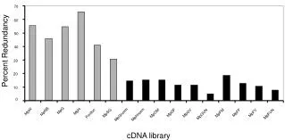
Download
1 / 58
590 likes | 614 Views
Detailed overview of the first MPW run by 3DIC Consortium, highlighting timeline, challenges encountered, design specifics, and the collaboration among members. Presentation given in March 2010.

E N D
3DIC Consortium MPW Run Review Jim Hoff and Ray Yarema Fermilab Marseille, France March 18, 2010 3DIC consortium meeting
Outline • MPW #1 time line • MPW run #1 submission summary • Problems encountered during submission process. 3DIC consortium meeting
Timeline • December 11, 2009 – first consortium meeting • Other consortium meetings – 2/09, 3/09, 5/09 • May ’09 all designs received by Fermilab • June ‘09 – March 4, 2010 – Files prepared and reviewed for submission numerous times. A large number of problems were discovered which needed to be corrected. (To be discussed in the last part of talk) • March 6, 2010- Fabrication begins by making first masks • ~ April 30- 2D wafers expected out of foundry • 3 wafers diced and parts sent to designers • Review needs of designers • Remaining wafers begin 3D assembly • ~ May 28, 3D wafers expected to be completed in Singapore • ~ June ’10 • 3D wafers diced and parts delivered to designers. • Review needs of designers • Full wafers delivered to appropriate institutions • Review needs of designers • Full wafers prepared for bump bonding at other facilities (Ziptronix) 3DIC consortium meeting
The First MPW Run • Initially, we at Fermilab thought we could assemble the MPW frame with all the designs. • Fermilab did not anticipate the complexity and number of problems to be uncovered and corrected. • We soon realized that it was impractical due to software and manpower limitations. • Tezzaron agreed to assemble the frame for us. • Tezzaron invested a great deal of extra time and manpower to keep our project moving forward and never gave up on us. • The MPW run submission always had the highest priority on the Fermilab ASIC work schedule • Sharing of special programs, such as fill, and design files benefited members of the consortium. 3DIC consortium meeting
Frame for First MPW Run • 3D chip has two tiers • One set of masks used for both top and bottom tiers to reduce mask cost. • Identical wafers bonded face to face by Tezzaron. • Backside metallization by Tezzaron. • Frame divided into 12 subreticules among consortium members • More than 25 two-tier designs (circuits and test devices) • CMS strips, ATLAS pixels • ILC pixels • B factory pixels • X-ray imaging • Test circuits • Radiation • Cryogenic operation • Via and bonding reliability • SEU tolerance 3DIC consortium meeting
MPW Full Frame Test chips: TX, TY 2.0 x 6.3 mm Notice Symmetry about vertical center line Subreticules: A, B, C, D, E, F, G, H, I, J 5.5 x 6.3 mm Top tiers Bottom Tiers 3DIC consortium meeting
Wafer Map and 3D Parts Count • 28 full reticules • 31 wafers • 25 for consortium, 3 of which are for 2D wafer testing • 6 for Fermilab • Max of 14 3-D assemblies • 3 for Fermilab • Remainder to be divided among all consortium members • Assume six working 3D wafers for consortium • 168 assemblies of each subreticule 3DIC consortium meeting
Frame Overview • The following slides are meant to present in one talk an overview of the designs in the various subreticules. • Details of the subreticules are not presented at this time but are left to the individual presenters for the different subreticules. • It is hoped each speakers will highlight the issues they encountered that are different or a problem when doing their 3D design. • Lack of desired tools. • Routing or shielding problems • Mirroring considerations • Restrictions imposed by 3D design such as: • Limited number of bond pads and predetermined locations between tiers. • Restricted bond pad spacing provided by Fermilab • Placement of vias • Fill/density requirements • Restrictions due to process options • Number of metal layers • MiM capacitors • Two top metal layers 3DIC consortium meeting
Subreticules A & B Highlights 1 1 2 2 3 A Left A Right B Left B Right • Subreticule A – Two subcircuits,intended to be bonded to sensors from XFAB ( 0.35 um with high Res EPI). An amplifier may be integrated in each sensor pixel • 1) ILC application (Strasbourg, Saclay) • Rolling shutter, low power tracker, 34 X 240 array, 20 um pitch pixels • Amp, Disc. & latch on analog tier, 1 bit memory& readout on digital tier • R.O. time=integration time (80 ns/row) • 2)ILC and bio-medical applications (Strasbourg, Bergamo, Pavia) • Self triggering pixel tracker, 245 x 245 array, 20 um pitch with fast X-Y projection readout • 2 sub arrays with different types of feedback caps in amplifier • ASD on analog tier, readout on digital tier • Subreticule B – Three subcircuits • 1) 2 separate memory cores(CMP) • one standard design and one with built-in SEL hardness circuitry • 2) MAPS for ILC(Scaly, Strasbourg) • 42x240 array, 20 um pixel MAPS operating in rolling shutter mode, • 80 ns/row • Sensor, amp, Disc & latch (NMOS only) on analog tier. 1 bit memory & readout on digital tier • 3) MAPS for ILC(Strasbourg) • 128 x192 array, 12x24 um pixel MAPS with 5 bit time stamp, 2nd hit marker, full serial readout • Future goal: to use separate sensor tier and to reduce the pixel size to 12x12 um. 3DIC consortium meeting
Subreticules C & D 1 2 1 2 3 3 4 Left Right Left Right • Subreticule C – 4 subreticules • 1) ATLAS 2D pixel design based on earlier design in IBM 0.13 um (FEI4)* (CPPM/Bonn) • Left (analog) side - 14 col, 60 rows, 50x166 um pixels with simple readout • Mating right side comprised of counter and “noisy” cells to study coupling to the left tier with different shielding ideas. • 2) SEU resistant register and TSV/bond interface daisy chain to measure TSV as well as bond yield. (CPPM) • 3) Test structures to evaluate transistor performance with TSVs in close proximity (CPPM) • 4) Test structures to test robustness of circuits under wire bond pads (CPPM) • Subreticule D – 3 subreticlues • 1) ATLAS 3D pixel design foreseen for ATLAS upgrade* (CPPM/Bonn) • Left (analog) side - 14 col, 60 rows, 50x166 um pixels (same as subreticule C) • Mating right side contains special features such as time stamp, time over threshold, and 4 pixel grouping. • 2) Small pixel array for SLHC* (LAL) • 24 x 64 array of 50 um pixels • ASD, threshold adjustment DAC/pixel, 24 DFF register/pixel • 3) TSV capacitance test circuits (CPPM) *Note: C1, D1, D2 are to be hybridized to sensors provided byHans-Gunther Moser, MPI 3DIC consortium meeting
4) Two test structures for the subreticule F DNW MAPS device (Pavia/Bergamo) • 16 x 16 array of 20 um pixels with inter-train sparsified readout • 8 x 8 array of 20 um pixels with selectable analog readout of each pixel • 5) Two 3D test structures • 3 x 3 array of 20 um pixels and 4 single channels for DNW MAPS (Pavia/Bergamo) • 3D RAPS structures including single ended I/O buffer, two single addressable 3T pixels with small and large area detecting diodes. • 5x 5 and 16 x 16 pixel matrices, each one featuring small and large detecting diodes (Perugia) • 6) 2D version of 3D MAPS device in subreticule F, 64 x64 array of 28 um pixels (Pavia/Bergamo) • 7) 2D sub-matrices with 10 and 20 um pixels to test signal to noise performance of MAPS in the Chartered process (Roma) Subreticules E & F 2 3 1 4 6 7 5 • Subreticule E – 7 sub-circuit areas • 1) 3D MAPS with 32 x 64 array of 25 um pixels with DCS, 3T FE, discriminator, auto-zeroing. All control logic in digital tier. (Roma) • 2) 3D MAPS test structures - Two 3 x 3 40um pitch arrays. One with shaperless preamplifiers. Other is designed with ELT input devices. (Pavia/Bergamo/Pisa) • 3) 3D MAPS test structure with 8 x 32 array of 40 um pixels, DNW sensors, data push architecture (Pavia/Bergamo/Pisa/Bologna) • Subreticule F – Pavia, Bergamo • 3D MAPS device with 256 x 240 array of 20 um pixels with DNW sensors and sparsification for ILC • The device may be tested with both a full thickness sensor substrate or with sensor thinned to 6 microns. 3DIC consortium meeting
Subreticules G & H • Subreticule G – Orsay/LBNL • ATLAS 2D pixel design based on earlier design in IBM 0.13 um (FEI4) • Left (analog) side - 14 col, 60 rows, 50x166 um pixels with simple readout • Analog tier designed for opposite polarity input from circuits in subreticules C and D. • Mating right side comprised of counter and “noisy” cells to study coupling to the left tier with different shielding ideas. • Top tier looks for hits from long phi strips and bottom tier looks for coincidence between phi strips and shorter Z strips connected to bottom tier. • Designed for 80 micron pitch sensors • Serial readout of all top and bottom strips along with coincidence information • Downloadable hit patterns • Fast OR outputs • Circuit to be thinned to 24 microns and connections made to both the top and bottom of the chip. • Subreticule H – FNAL/CPPM/LBNL – 3D chip (VICTR) used as a demonstrator for implementation of PT cut algorithm for tracker trigger in SCMS • Processes signals from 2 closely spaced parallel silicon strip sensor planes (phi and Z planes). 3DIC consortium meeting
Subreticules I & J • Subreticule I – FNAL – 3D demonstrator chip (VIP2b) for ILC vertex detector with separate bonded sensor • Adapted from earlier MIT LL designs in SOI technology • 192 x 192 array of 24 micron pixels • 8 bit digital time stamp • Data sparsification • DCS analog signal information output • Separate test input for every pixel cell • Serial output bus • Subreticule J – FNAL/AGH-UST/BNL – 3D demonstrator chip (VIPIC) for X-ray Photon Correlation Spectroscopy to be bonded to a separate sensor. • 64 x 64 array of 80 micron pixels • Separate Analog and digital tiers • Sparsified, binary readout • High speed frame readout • Optimized for 8 KeV photons • Triggerless operation • 16 Parallel serial output lines • Two 5 bit counters/pixel for dead timeless recording of multiple hits per time slice • Innovative binary tree pixel addressing scheme 3DIC consortium meeting
Test Chips TX & TY 1 2 1 2 TX Left TX Right TY Left TY Right • Subreticule TX • Test transistors for noise, radiation, and cryo measurements • 1) NMOS and PMOS transistor array with nominal Vt, low Vt, thick gate oxide I/O, 0 Vt, and 0 Vt thick gate oxide. Measured devices are thinned. (PAVIA) • 2) NMOS and PMOS transistor array with different numbers of fingers/transistor for measurements at cryo temperatures. Devices can be measured on thick or thin substrate.(FNAL) • 2) Test circuits for VIP2b in subreticule I – (FNAL) • Double correlated sampler • Single channel FE • Front ends with different W/L input transistors • Stand alone discriminator • Subreticule TY – (FNAL) • 1) Two long daisy chains of bond interconnects to measure interconnect yield. • Two different daisy chains having different bond interface patterns • Each daisy chain has 140000 bond interconnects with multiple taps • 2) Test transistors based on a standard set of devices (~46) used by CERN to characterize different processes. • Devices can be measured under different conditions • on standard wafers (2D wafers). • on thin substrate bonded to a thick second wafer • on thick substrate bonded to a thinned second wafer. 3DIC consortium meeting
Run Goals • This run should allow for evaluation of many factors • 3D processing • Affect of thinning and bonding on device performance • Yield of bond connections between tiers • Geometry of bond pads between tiers • Effect of vias near transistors • TSV capacitance and yield • Effect of bond pads over circuits • Digital coupling from one tier to another tier • Comparison of identical 2D and 3D designs in the same technology • Chartered process • Suitability of process for MAPS • Radiation tolerance and noise performance • Cryogenic performance/reliability • Performance of a large number of different circuits exploring many different operating conditions. • Establishment of guidelines for future submissions • Better understanding of the 3D design process 3DIC consortium meeting
The following slides will review some but not all the problems that were encountered when preparing this submission 3DIC consortium meeting
Introduction What follows is a list of some problems and mistakes that arose during the first Tezzaron 3D submission. These problems are listed in no particular order. Some were more significant than other. Some took more time than others. The purpose of this presentation is to help us understand the problems that arose and what had to be done to correct them. A second, equally important purpose of this paper is establish a design flow that will either eliminate or mitigate these problems on future designs. Please feel free to contribute. We would like to learn how these problems affected everyone. 3DIC consortium meeting
Submission Cycle 3DIC consortium meeting
Reticule Structure The original Frame Layout • Problem: • Chartered provided the maximum design area within the frame to Tezzaron who delivered it to Fermilab • We took into consideration Tezzaron’s target area and the 100um saw streets • We divided up the remaining area accordingly. • The result is the familiar diagram shown to the right. • The full frame was submitted with this floor plan. • This version was rejected because Chartered wanted space within the frame for PCMs 3DIC consortium meeting
Reticule Structure The second Frame Layout with a vertical street added for Chartered • Problem (continued): • The frame was then split vertically about the center line and the center saw street was left open for PCMs. This was done to preserve left right symmetry for 3D bonding and Ziptronix alignment marks already located in some streets. At this point there were open saw streets on both sides and one in the center. • A check was done again and the designs resubmitted • This submission was also rejected. Chartered still wanted more room. (The alignment key for each mask requires an area of 500um x 80um and there are many.) 3DIC consortium meeting
Reticule Structure The third Frame Layout with a two horizontal streets added at Chartered’s request • Problem (continued): • We changed the frame for the third time by opening two 80 um horizontal streets, once again leaving the street alignment marks in place for Ziptronix. • The resultant six piece reticule is shown at the right. • This frame was FINALLY acceptable. • All subsequent submissions to Chartered were broken into these 6 pieces. 3DIC consortium meeting
Final Tezzaron/Chartered Reticule Frame 3DIC consortium meeting The final Reticule Frame in some detail. 3 vertical streets and 4 horizontal streets 80um wide
General Reticule Frame Information • What is it? • Those parts of the reticule that are NOT part of a design • Who controls it? • Chartered. The sub-reticule information ultimately comes from us, but the Frame and the contents of the Streets come from Chartered. • What is in it? • All alignment keys and markers for 2D processing (Tezzaron’s markers are in their own “sub-reticule”) • All Process Control Monitors • Any extra alignment keys (or marker voids) we might need for follow-on 3D processing (e.g Ziptronix) • What did we learn from all this? • We should assume that at a minimum Chartered will need three vertical and two horizontal 80um wide open strips within the frame for PCMs (or the equivalent). • Follow-on processing might need to be cleared all the way up to Chartered because they control the streets. If we need to place some kind of targets or target voids in the streets, Chartered might want to say something about it. 3DIC consortium meeting
Design Kit Incompatibilities(Serious problems that were hard to find) Problem:Different Cadence/Calibre files were given to different 3D Consortium Members by different Chartered offices. Who had what? Who set their systems up properly? These problems were very hard to find. Experience has taught us to trust our tools and doubt our work (or the other guy’s work). When something goes wrong, we search for our own mistakes. Realizing it is in the tool takes a long time. 3DIC consortium meeting
Example #1:Different Stream Layer Map Tables A stream layer map test file sent out by Fermilab • Problem:Chartered has different processes with different numbers of metal layers, different transistors, different voltages, etc. These different processes have different stream layer numbers for the same layer name (e.g. Metal6 is 53 in processes where it is top metal but it has another layer number in other processes. Frankly, Chartered has a history of legacy problems with their evolving process lines.) • How we found it:We all began to notice it when we started to transfer files to one another. • What We Did This Time: • Sent out a test gds file (image on the right) • Some designs had to be re-worked • Long Term Solution:A single PDK from a single source. 3DIC consortium meeting
Example #2:Calibre Differences Problem:First of all, some of us were simply using different Calibre files. At least we were aware of it. However, even when we were using the same Calibre files, there were still problems. Chartered’s Calibre file reflects the large number of processes that it covers. In particular, we used 6 Metal Layers with 2 Top Metals. If this was not set up properly, different DRC rules were used. To make matters worse, Chartered’s Cadence PDK produced vias that were not compatible with Top (thick) Metal layers. A modification needed to be made to the Cadence Technology file by hand to fix this. How we found it:One design team used some of our standard cells on their design. They worked fine on their home computers, but when then submitted them to us, we noticed hundreds of design rule errors. It was obvious, at first, that they were using thin metal via4 structures. However, FERMILAB designed those via4 structures, and those same structures passed our DRC check. After much effort, it was determined that they were using a single top metal DRC file and that our modified via structure on their unmodified system was reverting to its thin metal dimensions. Long Term Solution:A single PDK from a single source. 3DIC consortium meeting
Undesirable layersin the Stream File The layers that are supposed to be in the stream file • Problem:This was a major problem that presented itself in several different ways over the course of the submission. • Several designs were submitted that contained layers that were not supposed to be there. • Since our DRC checkers concentrated on the layers that were supposed to be there, undesirable layers slipped through all the way to Chartered where they were caught by Chartered’s custom screening program • Several submissions cycles needed • These errors made us look bad 3DIC consortium meeting
Undesirable Stream Layers:Example 1 • Problem:Some designs used 2-Mask MiM Capacitors when they should have used 1-Mask MiM Capacitors • What it looked like to us (before Chartered told us what it was):Missing metal4 under a Via4. • What we did this time:The designs were sent back to the designers to be corrected. This problem cropped up again because a rework of one design did not fix all the errors and this was not discovered until the design reached Chartered again. 3DIC consortium meeting
Undesirable Stream Layers:Example 2 • Problem: Other designs used a high-resistance polysilicon resistor. • What it looked like to us (before Chartered told us what it was):Ordinary polysilicon • What we did this time:An extra mask layer was added to the processing so a re-design was not necessary. 3DIC consortium meeting
Undesirable Stream Layers:Solutions • Long Term Solutions: • Adequate communication of the process options • A complete understanding of the process options and • A complete adherence to the process options. • Other Possible Long Term Solutions: • A single Stream Layer Map Table available from a single source (Tezzaron or the 3DIC web site). • A perl script that scans the PIPO.LOG file and flags layers that do not belong. • A simple Calibre deck to search for erroneous layers and data types. 3DIC consortium meeting
Undesirable Stream Layers:Trimpl’s Submission Suggestion • Create a strict Stream layer map table that includes no text, pin, or polygon layers • Export a given design into a stream file using this layer map table • Re-import the stream file into Cadence using this layer map table, creating a copy of the original submission • Extract pin information from the original Cadence database and transfer it to the new copy. • Run LVS comparing the original schematics from the original database with the new copy of the layout. If the new layout matches the old schematic and if Tezzaron approves of the layer map table, then by definition, the stream file created in step 2 would contain only layers that are allowed by Tezzaron. Consortium Comments? 3DIC consortium meeting
TSV Problems (Part 1 - Structure) 0.5um Enclosed Super Contacts See Rule SC 2.1 • Problem:This was implemented using the “wrong” layer number (different stream layer map tables) although it is stated clearly as Tezzaron Rule (SC 2.1). TSV must be straddled by Metal1 and must overlap it by 0.5um. Failing to do so can release contaminants that can adversely affect subsequent VLSI processing steps. • How did we find it:Unrelated DRC checks revealed the problem • What We Did This Time: • Developed DRC checkers to find unprotected TSVs • Designs had to be sent back for re-work • Long Term Solution:Solved Problem. However, it must be included in future releases of the PDK. 3DIC consortium meeting
TSV Problems (Part 2 - Spacing) From Tezzaron’s SuperContact Rule PDF Min Max Rec. • Problem: • TSV spacing requirements are variable (see inset below) • Preferred is 100 x 1000 um. • Errors are flagged for spacing greater than 250 x 250 um. • IF there will be follow-on processing (e.g. Ziptronix, XFAB, etc), spacing should be tighter. • IF there are matching/analog requirements, spacing should be tighter. • Too wide and Tezzaron’s own 3D processing is adversely affected • Tezzaron’s Calibre deck (see previous slide) was checking a different layer number than some of us were using. However, once fixed, the rule remained max 250um, recommended 100um for uniformity of back-side etching (dishing) • Some of our members requested waivers. • How coarse could the spacing be before it affected neighbors? 3DIC consortium meeting
TSV Problems (Part 2 - Spacing) Too much space A bad TSV Spacing • What We Did This Time: • Developed DRC checkers to find TSV spacing • Designs had to be sent back for re-work • Long Term Solution: • Solved Problem • DRC Checkers must be incorporated into an official PDK release. 3DIC consortium meeting
Bond Interface The original Bond Interface with the original seal ring • Problem:Early bond interfaces had some problems. In particular, the density of the top metal in the seal ring region was an issue. • What We Did This Time: • With Tezzaron approval and numerous iterations, the final design was created. • Long Term Solution:Solved Problem. Fermilab is working on pCells for guard ring and seal ring as well as three basic bond interface configurations – basic, for designs with follow-on processing, and for design using their own characteristic step. 3DIC consortium meeting
Bond Interface The final Bond Interface with the final seal ring and guard ring The final seal ring alone • Problem:Early bond interfaces had some problems. In particular, the density of the top metal in the seal ring region was an issue. • What We Did This Time: • With Tezzaron approval and numerous iterations, the final design was created. • Long Term Solution:Solved Problem. Fermilab is working on pCells for guard ring and seal ring as well as three basic bond interface configurations – basic, for designs with follow-on processing, and for design using their own characteristic step. 3DIC consortium meeting
Bond Interface Uniformity and Gaps A custom bond interface Showing unacceptable gaps • Problem:When bond interfaces changed between regions, gaps were left between them were too large. • What We Did This Time: • Developed custom DRC check to look for gaps. • Sent the designs back to the designers for re-work. • In some cases Tezzaron inserted Octagons as needed by hand. • Long Term Solution:We have a check now. We all know about it and won’t do it again. In addition, Tezzaron has developed a bond interface insertion routine for Calibre. 3DIC consortium meeting
microMagic Software Bug #1 The standard bond interface at the Pixel level • microMagic is used by Tezzaron to assemble the frame • Problem: • Early submissions revealed errors on top metal (bond interface) during DRC checking. • Octagons close to the (0,0) point of a sub-reticule had no errors. Octagons further away had THOUSANDS . Unless the design was hierarchical. • Fermilab could not see these errors at all. Tezzaron could. • Was it a Calibre Version P (used by Fermilab) versus Version Q or R (used by Tezzaron) problem? No. • Visual inspection in Cadence was performed. Again, Fermilab could see nothing. Tezzaron could plainly see the problem. • Was this a Cadence (used by Fermilab) versus microMagic (used by Tezzaron )problem? Yes. 3DIC consortium meeting
microMagic Software Bug #1 The standard bond interface at the Pixel level • Problem:In the end, it was determined that microMagic’s gds import routine was rounding off locations of the octagon corners, placing them off grid • What We Did This Time:Had microMagic fix its own problem. • What they did was increase the number of significant bits in their rounding routine. • Long Term Solution:Problem solved 3DIC consortium meeting
microMagic Software Bug #2 Problem:Late in the design cycle, a “Minimum COMP Width” error was noticed in a single ARM cell in a single design. ARM cell errors had been ignored because Chartered, Tezzaron and Fermilab all “knew” that ARM cells were designable and other errors were far more significant. Once again:Tezzaron could see it. We could not. 3DIC consortium meeting
microMagic Software Bug #2 The errant ARM Cell : TLATXL 3DIC consortium meeting
microMagic Software Bug #2 Note the notch The errant ARM Cell : TLATXL There are quite a few grid points along this notch (13) All points of the COMP polygon are on grid Except these here. 3DIC consortium meeting
microMagic Software Bug #2 One could be generous and place part of the blame on ARM. It is somewhat sloppy to have off-grid polygons in a design. However, the points that were off-grid were insignificant to the overall design. Adjacent polygons overlapped the off-grid points making the overall structure continuous. No actual mask edge was off-grid. Cadence had no trouble with this at all because Cadence does not try to import onto its grid directly. Cadence permits off-grid structures. It is the DRC checkers that flag off-grid verticies. 3DIC consortium meeting
microMagic Software Bug #2 The errant ARM Cell as seen in microMagic after import : TLATXL 3DIC consortium meeting
microMagic Software Bug #2 The errant ARM Cell as seen in microMagic after import : TLATXL 3DIC consortium meeting
microMagic Software Bug #2 • Underlying Problem - microMagic: • Unlike Cadence, microMagic does try to import onto the grid (unless certain switches are used). • Off-grid vertices anywhere on the polygon triggered a grid approximation routine for all vertices of the polygon, even if those verticies were on already on-grid. • Apparently there is more to this algorithm than simple rounding or adjusting by +/- 1 grid point. • What We Did This Time : • Tezzaron developed a Calibre-based DRC check that compared your gds files to the files after microMagic import, strictly comparing layer to layer, square to square, and polygon to polygon. Any differences were flagged. There were many – e.g. targets, extra bond octagons, etc. However, ONLY the one ARM cell was found to be changed and it was used in only one sub-reticule. It was TLATXL from the ARM Library, and it was used in sub-reticule D • Tezzaron modified the design by hand and restored it to its original dimensions. • microMagic acknowledged this error and fixed it. • Long Term Solution:Solved Problem, we believe. 3DIC consortium meeting
Floating Metal (Metal1) 9 dummy TSVs • Problem:Chartered did not recognize TSVs as “connections”. Therefore, it saw our spacing/density related TSVs as floating metal1. • What We Did This Time:These were waived. • Long Term Solution: • Get Chartered to recognize TSVs as connections • Develop our software to recognize TSV connected metal1 as not floating. 3DIC consortium meeting
Floating Metal (Metal6) The standard bond interface at the Pixel level • Problem:The mechanical function of the bond interface meant that DRC checks of our designs showed thousands of floating metal 6 pieces • What We Did This Time:These were waived. • Long Term Solution: • Get Chartered to implement a dummy layer e.g. “bondInterface” to allow us to screen these errors. • Implement such a layer in our own design files. 3DIC consortium meeting
Floating Metal (“real”) An example of floating metal2 found by Chartered • Problem:In spite of the vast number of floating metal errors, Chartered still managed to find quite a number of “real” floating errors (i.e. could not be waived). • What we did this time: • Most of these errors were returned for re-work. • One (a floating bus) was fixed directly by Tezzaron with the designers permission 3DIC consortium meeting
Floating Metal (The Floating Bus) • Problem:There was a set of floating metal errors that were caused by a bus inserted into the design and then never used. This bus error was repeated many times in an array. • What we did: • Determined that the errors were actually the same error, repeated again and again. • Located a nearby ground strap • Tezzaron made a simple layout modification to connect the bus to the ground strap • Tezzaron performed a comprehensive, Calibre-based layout-versus-layout comparison between the original gds file submitted to Fermilab and the modified design. The designs matched indicating that the bus in question was truly floating and no essential change was made to the circuit. • Long Term Solutions: • Chartered is very strict when it comes to floating metals. It is possible, though this is just speculation, that they are particularly sensitive to floating metals in OUR designs because we have so many floating metals on metal1 and metal6. • It is also possible that the large number of waivable floating metals in our designs help to “hide” the un-waivable floating metals from our notice. • Prudence suggests that we implement the screening measures discussed in the previous slides, even if Chartered does not. 3DIC consortium meeting