Specifying Optical Components
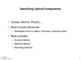
Specifying Optical Components. Lenses, Mirrors, Prisms,… Must include tolerances Allowable errors in radius, thickness, refractive index Must consider Surface defects Material defects Mounting features. Dimensional tolerances for lenses.

Specifying Optical Components
E N D
Presentation Transcript
Specifying Optical Components • Lenses, Mirrors, Prisms,… • Must include tolerances • Allowable errors in radius, thickness, refractive index • Must consider • Surface defects • Material defects • Mounting features J. H. Burge University of Arizona
Dimensional tolerances for lenses Diameter tolerance of 25 ± 0.1 mm means that the lens must have diameter between 24.9 and 25.1 mm Lens thickness is almost always defined as the center thickness Typical tolerances for small (10 - 50 mm) optics: Diameter +0/-0.1 mm Thickness ± 0.2 mm Clear aperture is defined as the area of the surface that must meet the specifications. For small optics, this is usually 90% of the diameter. J. H. Burge University of Arizona
Understanding wedge in a lens • “wedge” in a lens refers to an asymmetry between • The “mechanical axis”, defined by the outer edge. • And the “optical axis” defined by the optical surfaces Lens wedge deviates the light, which can cause aberrations in the system J. H. Burge University of Arizona
Optical vs. Mechanical Axis R2 R1 Decenter is the difference between the mechanical and optical axes (may not be well defined) J. H. Burge University of Arizona
Effect of lens wedge • = ETD / D d = a(n – 1) J. H. Burge University of Arizona
Tilt and decenter of lens elements Parks J. H. Burge University of Arizona
Specifying wedge in a lens • The optical axis of a lens defined by line connecting centers of curvature of the optical surfaces • The mechanical axis defined by outer edge, used for mounting. • Wedge angle a = Edge Thickness Difference (ETD)/Diameter (often converted to minutes of arc) • Deviation d = (n-1)*a • Lenses are typically made by polishing both surfaces, then edging. The lens is held on a good chuck and the optical axis is aligned to the axis of rotation. Then a grinding wheel cuts the outer edge. • The wedge specification dictates the required quality of the equipment and the level of alignment required on the edging spindle. • Typical tolerances are • 5 arcmin is easy without any special effort • 1 arcmin is readily achievable • 15 arcsec requires very special care J. H. Burge University of Arizona
f Optical axis Mechanical axis deviation d decenter s Wedge a Lens element centration • Lens wedge can also be describe as centration. This is defined as the difference between the mechanical and optical axes. J. H. Burge University of Arizona
Centering a lens 1. Use optical measurement J. H. Burge University of Arizona
Centering a lens • Use mechanical measurement 1. Move lens until dial indicator does not runout 2. Measure Edge runout If the edge is machined on this spindle, then it will have the same axis as the spindle. J. H. Burge University of Arizona
Specification of lens tilt J. H. Burge University of Arizona
Automatic edging Clamped between two chucks with common axis, then outer edge is ground concentric. J. H. Burge University of Arizona
Edge bevels • Glass corners are fragile. Always use a bevel unless the sharp corner is needed (like a roof). If so, protect it. J. H. Burge University of Arizona
Rules of thumb for edge bevels Nominally at 45° J. H. Burge University of Arizona
Tolerancing of optical surfaces • Radius of curvature Tolerance on R (0.2% is typical) Tolerance on sag (maybe 3 µm = 10 rings) • Conic constant (or aspheric terms) • Surface form irregularity (figure) • Surface texture (finish) • Surface imperfections (cosmetics, scratch/dig) • Surface treatment and coating } PSD = A/f B Get nominal tolerances from fabricator J. H. Burge University of Arizona
Tolerance for radius of curvature Surface can be made spherical with the wrong radius. Tolerance this several ways: • Tolerance on R (in mm or %) • Tolerance on focal length (combines surfaces and refractive index) • Tolerance on surface sag (in µm or rings) 1 ring = l/2 sag difference between part and test glass J. H. Burge University of Arizona
Test plates • Most optical surfaces are measured against a reference surface called a test plate • The radius tolerance typically applies to the test plate • The surface departure from this will then be specified i.e. 4 fringes (or rings) power, 1 fringe irregularity • The optics shops maintain a large number of test plates. It is economical to use the available radii. • Optical design programs have these radii in a data base to help make it easy to optimize the system design to use them. Your design can then use as-built radii. • If you really need a new radius, it will cost ~$1000 and 2 – 3 weeks for new test plates. You may also need to relax the radius tolerance for the test plates. J. H. Burge University of Arizona
Test plate measurement Power looks like rings Irregularity Interferogram Phase map J. H. Burge University of Arizona
Surface figure specification • Wavefront error = Surface error • Specifications are based on measurement • Inspection with test plate. Typical spec: 0.5 fringe = l/4 P-V surface • Measurement with phase shift interferometer. Typical spec: 0.05 l rms • For most diffraction limited systems, rms surface gives good figure of merit • Special systems require Power Spectral Density specPSF is of form A/fB • Geometric systems really need a slope spec, but this is uncommon. Typically, you assume the surface irregularities follow low order forms and simulate them using Zernike polynomials – rules of thumb to follow… J. H. Burge University of Arizona
Wavefront error vs Image shape ex, ey are errors in ray position at focal plane Wi is wavefront error from surface i are wavefront slope errors (dimensionless) Bi is diameter of beam footprint from single field point (< diameter of the element) FN is system focal ratio For each ray: J. H. Burge University of Arizona
Surface irregularity For 1 µm P-V surface irregularity: Rules of thumb Exact dependence is functionof the form of the error 1 for < 2” optics 2 for > 6” optics Normalize slopes to µm/radius where the radius = half of the diameter. J. H. Burge University of Arizona
Effect of surface irregularity – rms wavefront DW, the wavefront error from surface error DS is Where n is the refractive index (use n = -1 for reflection) fis the angle of incidence Define ai = ratio of beam footprint from single field point to the diameter of optic = B/D For spherical surfaces like lenses, wavefront errors for each field point will fall off roughly with a, so surface i would contribute a wavefront error of J. H. Burge University of Arizona
Effect on system wavefront due to surface irregularity from lenses Using rules of thumb for 1 l P-V glass surfaces, l = 0.5 µm, n = 1.5, cosf = 1: Gives a wavefront contribution of DW = 0.125a waves rms per surface For M lenses (2 surfaces per lens) with 1 wave P-V surfaces and average a of 0.7, the overall wavefront error will be roughly evaluating A lens with 4 elements will have wavefront errors of about 0.25 waves rms (~20% SR, NOT diffraction limited) J. H. Burge University of Arizona
Effect of surface irregularity, rms spot size 1. Convert the normalized surface slope Q to wavefront slope Surface slope (µm/radius) Convert slope to units of µm/mm by dividing by the lens radius Convert to wavefront • Relate rms wavefront slope to rms spot size (via Optical Invariant) Bi =aiDi = beam footprint from single field point Fn is system working focal ratio Where erms gives the image degradation in terms of rms image radius. Di is the lens diameter, Bi = aiDi is the diameter of the beam from a single field point. J. H. Burge University of Arizona
Effect on system spot size to surface irregularity from lenses Using rules of thumb for 1 l P-V glass surfaces for small lenses, l = 0.5 µm, n = 1.5, cosf = 1: Qrms, rms surface slope error, is 1 waves/radius = 0.5 µm/radius rms evaluating For M lenses (2 surfaces per lens) with 1 wave P-V surfaces and average a of 0.7, the overall wavefront error will be roughly So the 1 l P-V surfaces from an f/8 lens with 4 elements would cause 8 µm rms blur in the image. This is about 2 times larger than the effect of diffraction. J. H. Burge University of Arizona
Power Spectral Density High performance systems use PSD to specify allowable surface errors at all spatial frequencies PSD typically shows mean square surface error as function of spatial frequency. Get rms in a band by integrated and taking the square root Typical from polishing: PSD = A * f-2 (not valid for diamond turned optics) (for 1-m optic) J. H. Burge University of Arizona
Surface roughness • Small scale irregularity (sometimes called micro-roughness) in the surface, comes from the polishing process. • Pitch polished glass, 20 Å rms is typical • Causes wide angle scatter. Total scatter is s2, where s is rms wavefront in radians. • Example: for a 20 Å lens surface -> 10 Å wavefront, for 0.5 µm light, s is 0.0126 rad. Each surface scatters 0.016% into a wide angle Typical data for a pitch polished surface J. H. Burge University of Arizona
Effect of small scale errors Consider figure errors of DS nm rms with spatial period L Convert to wavefront, and to radians s2 of the energy is diffracted out of central core of point spread function Diffraction angle qis ±l/ L (wherel is wavelength) For L<<D Optical Invariant analysis tells us that the effect in the image plane will be energy at aDi is the beam diameter from a single field point on surface i under consideration Fn is the system focal ratio Each satellite image due to wavefront ripples has energy s2/2 of the main image J. H. Burge University of Arizona
Surface Imperfections Surface defects are always present at some level in optical surfaces. These consist of scratches, digs (little pits), sleeks (tiny scratches), edge chips, and coating blemishes. In most cases these defects are small and they do not affect system performance. Hence they are often called “beauty specifications”. They indicate the level of workmanship in the part and face it, nobody wants their expensive optics to looks like hell, even if appearance does not impact performance. In most cases surface defects only cause a tiny loss in the system throughput and cause a slight increase in scattered light. In almost all cases, these effects do not matter. There are several cases that the surface imperfections are more important – • Surfaces at image planes. The defects show up directly. • Surfaces that must see high power levels. Defects here can absorb light and destroy the optic. • Systems that require extreme rejection of scattered light, such as would be required to image dim objects next to bright sources. • Surfaces that must have extremely high reflectance, like Fabry-Perot mirrors. J. H. Burge University of Arizona
Scratch Dig spec The specification of surface imperfections is complex. The most common spec is the scratch/dig specification from MIL-O-13830A. Few people actually understand this spec, but it has become somewhat of a standard for small optics in the United States. A related spec is MIL-C-48497 which was written for reflective optics, but in most cases, MIL-O-13830 is used. Mil-O-13830A is technically obsolete and has been replaced by Mil-PRF-13830B. A typical scratch/dig would be 60/40, which means the scratch designation is 60 and the dig designation is 40 The ISO 10110 standard makes more sense, but it has not yet been widely adopted in the US. J. H. Burge University of Arizona
Scratch spec per Mil-O-13830A Specification of surface defects per MIL-O-13830A Scratch/Dig Scratch designation N : measured by comparing appearance with standard scratches under controlled lighting Calculated as indicated -- For scratches designated as n1, n2 , ... length l1, l2, ... Part diameter (or effective diameter) D 1. Combined length of scratches of type N must not exceed D/4 2. If a scratch designated N is present, sum(ni * li)/D must be not exceed N/2 3. If no scratch designated N is present, sum(ni * li)/D must be not exceed N Example: J. H. Burge University of Arizona
Dig spec per Mil-O-13830A / Mil-PRF-13830B A dig is a small pit in the surface. Originates from defect in the material or from the grinding process. Dig designation M = actual diameters in µm / 10 1. Number of maximum digs shall be one per each 20 mm diameter on the optical surface. 2. The sum of the diameters of all digs shall not exceed 2*M (Digs less than 2.5 µm are ignored). 3. For surfaces whose dig quality is 10 or less, digs must be separated by at least 1 mm. J. H. Burge University of Arizona
Rules of thumb for lenses Base: Typical, no cost impact for reducing tolerances beyond this. Precision: Requires special attention, but easily achievable in most shops, may cost 25% more High precision: Requires special equipment or personnel, may cost 100% more J. H. Burge University of Arizona
Tolerancing for optical materials • Refractive index value • Dispersion • Refractive index inhomogeneity • Straie • Stress birefringence • Bubbles, inclusions Get nominal tolerances from glass catalogs Some glasses and sizes come in limited grades. J. H. Burge University of Arizona
Refractive index tolerance • The actual glass will depart from the design value by some amount. Use melt sheet from the actual batch of glass for improved accuracy. • The effect of refractive index errors is determined by perturbation analysis. • From Schott: Tolerances of Optical Properties consist of deviations of refractive index for a melt from values stated in the catalog. Normal tolerance is ±0.001 for most glass types. Glasses with nd greater than 1.83 may vary by as much as ±0.002 from catalog values. Tolerances for nd are ±0.0002 for Grade 1, ±0.0003 for Grade 2 and ±0.0005 for Grade 3. The dispersion of a melt may vary from catalog values by ±0.8%. Tolerances for vd are ±0.2% for Grade 1, ±0.3% for Grade 2 and ±0.5% for Grade 3. J. H. Burge University of Arizona
Internal glass variations J. H. Burge University of Arizona
Effects of index variations • Straie are small scale. Small amounts of straie have similar effects as cosmetic surface errors • Beware, unselected glass can have large amounts of straie • Refractive index inhomogeneity happens on a larger scale. The wavefront errors from an optic with thickness t and index variation Dn are DW = t * Dn • Use the same rules of thumb for surfaces to get rms and slopes. Example: A 25-mm cube beamsplitter made from H1 quality glass. Dn = ±2E-5, (4E-5 P-V, 1E-5 or 10 ppm rms ). DW = (25-mm)*(10 ppm rms) = 250 nm rms, this is l/2 rms for 500 nm wavelength. J. H. Burge University of Arizona
Effects of birefringence • Birefringence is a result of internal stress in the glass. This is minimized by fine annealing (slow cooling). • Birefringence is observed in polarized light • Large amounts of birefringence indicate large stress, which may cause the part to break • The retardance due to the birefingence can be estimated as Retardance = birefringence * thickness/ wavelength So the 25 mm cube beamsplitter with 10 nm/cm birefringence will cause 25 nm or about lambda/20 retardance J. H. Burge University of Arizona
Bubbles and inclusions The characterization of the bubble content of a glass is done by reporting the total cross section in mm2 of a glass volume of 100 cm3, calculated from the sum of the detected cross section of bubbles. Inclusions in glass, such as stones or crystals are treated like bubbles of the same cross section. The evaluation considers all bubbles and inclusions >0.03 mm. Bubbles have effects similar to surface digs. Usually they are not important. (Ref. Schott catalog) J. H. Burge University of Arizona
Rules of Thumb for glass properties J. H. Burge University of Arizona (Ref. Schott catalog)
Chemical resistance of optical glasses From Schott Glass: Climate resistance (CR) is a test that evaluates the material’s resistance to water vapor. Glasses are rated and segregated into classes, CR 1 to CR 4. The higher the class, the more likely the material will be affected by high relative humidity. In general, all optically polished surfaces should be properly protected before storing. Class 4 glasses should be processed and handled with extra care. Resistance to acid (SR) is a test that measures the time taken to dissolve a 0.1µm layer in an aggressive acidic solution. Classes range from SR 1 to SR 53. Glasses of classes SR 51 to SR 53 are especially susceptible to staining during processing and require special consideration. Resistance to alkali (AR) is similar to resistance to acid because it also measures the time taken to dissolve a 0.1µm layer, in this case, in an aggressive alkaline solution. Classes range from SR 1 to SR 4 with SR 4 being most susceptible to stain from exposure to alkalis. This is of particular interest to the optician because most grinding and polishing solutions become increasingly alkaline due to the chemical reaction between the water and the abraded glass particle. For this reason most optical shops monitor the pH of their slurries and adjust them to neutral as needed. Resistance to staining (FR) is a test that measures the stain resistance to slightly acidic water. The classes range from FR 0 to FR 5 with the higher classes being less resistant. The resultant stain from this type of exposure is a bluish-brown discoloration of the polished surface. FR 5 class lenses need to be processed with particular care since the stain will form in less than 12 minutes of exposure. Hence, any perspiration or acid condensation must be removed from the polished surface immediately to avoid staining. The surface should be protected from the environment during processing and storage. J. H. Burge University of Arizona
Conventions, standards,… • There now exists international standards for specifying optical components. ISO-10110. • The ISO standards provide a shortcut for simplifying drawings. When they are used correctly, they allow technical communication across cultures and languages • Use ISO 10110 --- Optics and Optical InstrumentsPreparation of drawings for optical elements and systems, A User’s Guide 2nd Edition, by Kimmel and Parks. Available from OSA. • The ISO standards are not widely used in the US, and will not be emphasized in this class. J. H. Burge University of Arizona
ISO 10110 --- Optics and Optical InstrumentsPreparation of drawings for optical elements and systems • 13 part standard • 1. General • 2. Material imperfections -- Stress birefringence • 3. Material imperfections -- Bubbles and inclusions • 4. Material imperfections -- Inhomogeneity and striae • 5. Surface form tolerances • 6. Centring tolerances • 7. Surface imperfection tolerances • 8. Surface texture • 9. Surface treatment and coating • 10. Tabular form • 11. Non-toleranced data • 12. Aspheric surfaces • 13. Laser irradiation damage threshold • available from ANSI 212-642-4900 • Better yet, User’s Guide is available from OSA J. H. Burge University of Arizona
ISO 10110 --- Optics and Optical InstrumentsPreparation of drawings for optical elements and systems • Codes for tolerancing 0/A Birefringence, A is max nm/cm OPD allowed 1/N x A Bubbles and inclusions, allowing N bubbles with area A 2/A;B Inhomogeneity class A, straie class B 3/A(B/C) sagitta error A, P-V irregularity B, zonal errors C (all in fringes) 4/s s is wedge angle in arc minutes 5/N x A Surface imperfections, N imperfections of size A CN x A Coating imperfections, N imperfections of size A LN x A Long scratches, N scratches of width A µm EA Edge chips allowed to protrude distance A from edge 5/TV Transmissive test, achieving visibility class V 5/RV Reflective test, achieving visibility class V 6/H Laser irradiation energy density threshold H J. H. Burge University of Arizona
Drawing example per ISO 10110 J. H. Burge University of Arizona
Standards General, physical dimensions ISO-10110-1 Optics and optical instruments – Preparation of drawings for optical elements and systems – Part 1: General ISO-10110-6 Optics and optical instruments – Preparation of drawings for optical elements and systems – Part 6: Centring tolerances ISO-10110-10 Optics and optical instruments – Preparation of drawings for optical elements and systems – Part 10: Tabular form ANSI Y14.5M Dimensioning and tolerancing ISO 7944 Reference wavelength ISO 128 Technical drawings – General principles of presentation ISO 406, Technical drawings – Tolerancing of linear and angular dimensions ISO 1101, Technical drawings – Geometrical tolerancing – form, orientation, run-out ISO 5459, Technical drawings – Geometrical tolerancing – datums and datum systems ISO 8015, Technical drawings – Geometrical tolerancing – fundamental tolerancing principle for linear and angular tolerances DIN 3140 Optical components, drawing representation figuration, inscription, and material. German standard, basis of ISO 10110 MIL-STD-34 Preparation of drawings for optical elements and systems: General requirements, obsolete ANSI Y14.18M Optical parts Optical surfaces ISO-10110-5 Optics and optical instruments – Preparation of drawings for optical elements and systems – Part 5: Surface form tolerances ISO-10110-7 Optics and optical instruments – Preparation of drawings for optical elements and systems – Part 7: Surface imperfection tolerances ISO-10110-8 Optics and optical instruments – Preparation of drawings for optical elements and systems – Part 8: Surface texture ISO-10110-12 Optics and optical instruments – Preparation of drawings for optical elements and systems – Part 12: Aspheric surfaces MIL-HDBK-141 MIL-STD-1241 Optical terms and definitions Mil-O-13830A, Optical components for fire control instruments; General specification governing the manufacture, assembly, and inspection of. ANSI PH3.617, Definitions, methods of testing, and specifications for appearance imperfections of optical elements and assemblies ISO 4287 Surface roughness – Terminology ISO 1302 Technical drawings – Method of indicating surface texture on drawings ANSI Y14.36 Engineering drawing and related documentation practices, surface texture symbols J. H. Burge University of Arizona
More Standards Material imperfections ISO-10110-2 Optics and optical instruments – Preparation of drawings for optical elements and systems – Part 2: Material imperfections – stress birefringence ISO-10110-3 Optics and optical instruments – Preparation of drawings for optical elements and systems – Part 3: Material imperfections – bubbles and inclusions ISO-10110-4 Optics and optical instruments – Preparation of drawings for optical elements and systems – Part 4: Material imperfections – inhomogeneity and striae MIL-G-174 Military specification – Optical glass Coatings ISO-10110-9 Optics and optical instruments – Preparation of drawings for optical elements and systems – Part 9: Surface treatment and coating ISO 9211-1, Optics and optical instruments – Optical coatings – Part 1: Definitions ISO 9211-2, Optics and optical instruments – Optical coatings – Part 2: Optical properties ISO 9211-3, Optics and optical instruments – Optical coatings – Part 3: Environmental durability ISO 9211-4, Optics and optical instruments – Optical coatings – Part 4: Specific test methods MIL-C-675 Coating of glass optical elements MIL-M-13508 Mirror, front surface aluminized: for optical elements MIL-C-14806 Coating, reflection reducing, for instrument cover glasses and lighting wedges MIL-C-48497 Coating, single or multilayer, interference, durability requirements for MIL-F-48616 Filter (coatings), infrared interference: general specification for J. H. Burge University of Arizona
Even more standards Measurement, inspection, and test ISO 9022: Environmental test methods ISO 9039: Determination of distortion ISO 9211-4, Optics and optical instruments – Optical coatings – Part 4: Specific test methods ISO 9335: OTF measurement principles and procedures ISO 9336: OTF, camera, copier lenses, and telescopes ISO 11455: OTF measurement accuracy ISO 9358: Veiling glare, definition and measurement ISO 9802: Raw optical glass, vocabulary ISO 11455: Birefringence determination ISO 12123: Bubbles, inclusions; test methods and classification ISO 10109: Environmental test requirements ISO 10934: Microscopes, terms ISO 10935: Microscopes, interface connections ISO 10936: Microscopes, operation ISO 10937: Microscopes, eyepiece interfaces ASTM F 529-80 Standard test method for interpretation of interferograms of nominally plane wavefronts ASTM F 663-80 Standard practice for manual analysis of interferometric data by least-squares fitting to a plane reference surface ASTM F 664-80 Standard practice for manual analysis of interferometric data by least-squares fitting to a spherical reference surface and for computer-aided analysis of interferometric data. ASTM F 742-81 Standard practice for evaluating an interferometer MIL-STD-810 Environmental test methods J. H. Burge University of Arizona
References • D. Anderson and J. Burge, “Optical Fabrication,” in Handbook of Optical Engineering, (Marcel Dekker, New York, 2001). • R. K. Kimmel and R. E. Parks, ISO 10110 --- Optics and Optical Instruments Preparation of drawings for optical elements and systems, A User’s Guide 2nd Edition, Available from OSA. • Earle, J. H., Chap 21 “Tolerancing” in Engineering Design Graphics (Addison-Wesley, 1983) • Foster, L. W., Geometrics III, The Application of Geometric Tolerancing Techniques, (Addison-Wesley, 1994) • Parks, R. E. “Optical component specifications” Proc. SPIE 237, 455-463 (1980). • Plummer, J. L. , “Tolerancing for economics in mass production optics”, Proc. SPIE 181, 90-111 (1979) • Thorburn, E. K., “Concepts and misconceptions in the design and fabrication of optical assemblies,” Proc. SPIE 250, 2-7 (1980). • Willey and Parks, “Optical fundamentals” in Handbook of Optical Engineering, A. Ahmad, ed. (CRC Press, Boca Raton, 1997). • Willey, R. R. “The impact of tight tolerances and other factors on the cost of optical components,” Proc. SPIE 518, 106-111 (1984). • Yoder, P., Opto-Mechanical Systems Design, (Marcel Dekker, 1986). • R. Plympton and B. Weiderhorn, “Optical Manufacturing Considerations, “ in Optical System Design by R. E. Fischer and B. Tadic-Galeb, published by SPIE Press and McGraw-Hill. • Schott Glass • Ohara Glass Catalog • Hoya Glass Catalog J. H. Burge University of Arizona