Download
1 / 24
240 likes | 424 Views
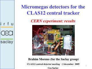
Micromegas Bulk for CLAS12 vertex tracker. Micromegas for CLAS12. Micromegas (MM) as central tracker for the CLAS12 experience at Jlab in 2014 CAD Study and remote electronic Curved Bulk prototyping and tests Saclay bulk test 2007 CERN Prototyping and tests in Saclay 2008

E N D
Micromegas for CLAS12 Micromegas (MM) as central tracker for the CLAS12 experience at Jlab in 2014 CAD Study and remote electronic Curved Bulk prototyping and tests Saclay bulk test 2007 CERN Prototyping and tests in Saclay 2008 MGPD in 5T field Lorentz angle study and test First curved: Saclay 2005
Vertex trackerwhy Gaseous, compared to Si ? • Less material (~.0015 LR) • Larger ΔR → same intrinsic momentum and angle resolution for less channels • smaller dead zones • Cheaper • Resistant: “immortal while breathing”
Bulk tracker Project for CLAS12 at Jlab Mixed solution: Silicium + Micromegas bulk • Central detector • 2 planes of Silicium (X,Y) • 3 cylindrical bulks (XY): 3m2, pitch 0.6 mm ,10k channels. • Forward detector • 4 plane bulks (XY): 1 m2, 3k channels. Cylindrical bulks Silicium beam target FVT 600 mm for F 500 mm
Mechanical & electronic implantation ? A CAD study was done with curved detectors. 3 double, X and Y strips at 90°, cylinders around the target with a 3 double end cap. Conclusion: • Mechanical implantation possible • Curved detector for “Y strip” • Electronic needs to be remote “As Far As Possible” (compass: 300 mm) • Test done on long kapton braid • Study of a ad hoc ASIC for tracker to be decide
3D remote-elec. model • Good solution to be validated with long (> 800 mm) electronics braids
Saclay Bulk Lab (2007) The Detector are made in a bulk lab using PCB machines design for university. The ability to realize the bulk allowed fast R&D with several configuration The thin PCB is transformed in bulk flat and then curved. • PCB used: • FR4 from 60 to 200 micron • Kapton 25 to 100 micron • mesh used: • Woven wire 19 micron
First curved bulk (09-2006) • PCB: 100 µm FR4 with 5 µm thick Cu strip • 100 µm amplification gap • Woven Mesh Gantois non stretched bulk with an array of 400 µm pillar every 2 mm • Dimension: 180 mm x 60 mm Picture: bulk curved, 100 mm radius
First prototype test 1er Fe55pick on a curved bulk E/E ~ 40% vs 25% on thick bulk 15 proto realize, 14 tested Study for drift pillar
Thin bulk micromegasPrototype made at CERN (2008) • Thin bulk (15 x 10-4 LR), long (600 mm) detector with a remote (800 mm) ASIC (AFTER)
PLV1 curved tests • One prototype was curved on a Y structure. We obtained a good gain homogeneity and E resolution degrade to 40%. Drift integration Before drift integration Under test
Curved bulk integration • Issue to be solved • Temperature curing during bulk fabrication process: differential thermal dilatation on thin PCB • Tension on the mesh vs. curvature • Sealed drift • A 100 µm aluminize mylar is silicon glued with a 2 mm thick silicon join on the PCB. Gaz capillary tube glued either on drift or on PCB
Gain on curved bulk First test under way, similar gain behavior with small increases depending of curvature.
Before curvature energy calibration Energy resolution
Curved bulk energy resolution Energy resolution degraded due to in-homogeneity in the amplification gap. 38.8 % FWHM versus 20% flat mesh pcb • Possible solution: • Nylon/metal mesh • Curved process
Flexible cable measurement Different flex PCB cable were realise at CIRE/SPCI: • Strip cables (40cm, 80cm et 80cm U-shaped) • Wire cables (40 cm, 80cm et 80 cm U-shaped) Noise and crosstalk measurement test were conclusive for 800 mm. Flex PCB cable, 80 cm U-shaped Acquisition made with T2K Labview DAQ Software
AFTER signal on the strips Channel 71 ADC 55Fe shaped signal Signal Signal - noise Noise 512 time samples Time (x 50 ns)
Noise study: preliminary results Pedestal for channel 71
Gaseous detector in 5T field ? • Magnetic environment to deal with : 5 T orthogonal to the detector ! tanθ = v x B / E Standard conditions : E= 1 kV/cm, v= 8 cm/μsec θ = 75 ° Adapted conditions: E= 10 kV/cm, v= 5 cm/μsec θ = 14° e-
Lorentz angle behaviour with the magnetic field B = 0T • Lorentz angle mesured from the deviation of the B=0T peak • Drift distance: 2.25mm • The signal spreads out with the Lorentz deviation → increase the resolution B = 1.5T Labview DAQ
Test at 5T • Test done at Jlab on the DVCS magnet. • The prototype is fixed on a mobile cart (telescopic slide rail) itself fixed on the magnet. • The handcart allows full test in and out without dismounting the detector. Will be used for future test @ 5T with DVCS magnet. 400 mm In Out
Curved bulk demonstrator Cylindrical prototype Magnet interface (3 Teflon pads) X tile Y cylinder Length: 600 mm Diameter: 180 / 220 mm 1728 Channels Y joint Y connector Y HT cable Interface attachment to handcart