Download
1 / 31
310 likes | 511 Views
Cross Sectional View of FET. FET I-V Characteristic. Saturation Voltage. V pinchoff = V DS,sat = V GS – V TH Separates resistive from saturation region The drain current is given by Solving for V DS,sat :. Early Voltage Function of Length. Early Voltage in MOSFETs.

E N D
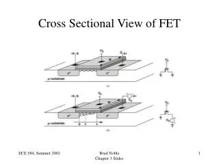
Cross Sectional View of FET Brad Noble Chapter 3 Slides
FET I-V Characteristic Brad Noble Chapter 3 Slides
Saturation Voltage • Vpinchoff = VDS,sat = VGS – VTH • Separates resistive from saturation region • The drain current is given by • Solving for VDS,sat: Brad Noble Chapter 3 Slides
Early Voltage Function of Length Brad Noble Chapter 3 Slides
Early Voltage in MOSFETs • Due to channel length modulation: • Good to solve for quiescent voltage-current. Brad Noble Chapter 3 Slides
Ex: Find VDS,sat for an NFET Brad Noble Chapter 3 Slides
Body Effect Brad Noble Chapter 3 Slides
Cox Gate oxidecapacitance inversionlayer Depletion cap,function of x Cdep Variations in VTHAcross Channel • We assume VTH is constant across channel THIS IS NOT TRUE! • Depletion region is thick at S and thin at D. Brad Noble Chapter 3 Slides
Small Signal Equivalent Ckt Brad Noble Chapter 3 Slides
Parasitic Capacitance Brad Noble Chapter 3 Slides
Capacitance Equivalent Circuit Brad Noble Chapter 3 Slides
Variation in Capacitance Brad Noble Chapter 3 Slides
Notes on PFETs • PFETs typically have a shape factor 3 or 4 times larger than NFETs • Body effect can be eliminated in PFETs by tying the n-well to VDD • Need 6m spacing between n-wells to isolate. • Dr. Engel always does this on input devices, not always elsewhere. Brad Noble Chapter 3 Slides
Subthreshold Conduction Brad Noble Chapter 3 Slides
Weak Inversion • What really happens if VGS < VTN? • In digital design, IDS = 0. • We call it “weak inversion” or W.I. • IDS is primarily due to Idrift in strong inversion and Idiffusion in weak inversion. Brad Noble Chapter 3 Slides
Modes of Inversion • IDS = Idrift + Idiffusion • If VGS > VTN the channel has been inverted. • To be more precise, we can say the channel has been “strongly inverted” (S.I.) due to an abundance of carriers in the channel. • Inversion is independent of whether the FET is in the linear or saturation region. Brad Noble Chapter 3 Slides
Weak Inversion Idiffusion • Drain is more reverse biased than source: • To find Idiff, compute gradient • Because no carriers are lost as they travel from S to D, current is the same for all x and gradient is not a function of x. • Note: This is not really true due to recombination, but its close! Brad Noble Chapter 3 Slides
W.I. Surface Potential Brad Noble Chapter 3 Slides
Deriving Weak Inversion IDS Brad Noble Chapter 3 Slides
W.I. FET As Exp. Law Dev. • S must be big for device to be useful. • If VDS = 100mV, can be neglected. • For W.I. vDS,Sat 100mV • Looks like a BJT Brad Noble Chapter 3 Slides
Inversion Coefficient • Let • Shape factor as a function of : Lets you chose shape to match inversion mode. Brad Noble Chapter 3 Slides
Ex. Using Inversion Coeff. Brad Noble Chapter 3 Slides
Small Signal Analysis Brad Noble Chapter 3 Slides
Ex: Quiescent Point Question: How many digits are significant? Brad Noble Chapter 3 Slides
Small Signal Model Limits • Suppose the previous circuit is the input device of an amplifier. • Small-signal model holds as long as the deviations are small Brad Noble Chapter 3 Slides
Taylor Series Expansion • Taking a Taylor expansion of one variable: Brad Noble Chapter 3 Slides
Small Signal Model Params Brad Noble Chapter 3 Slides
Example: Small Signal Analysis Brad Noble Chapter 3 Slides
Small Signal Low-Freq Model Brad Noble Chapter 3 Slides
Ex: Find gm and rO Brad Noble Chapter 3 Slides
Transconductance: W.I. & M.I. • What is gm for a weakly inverted FET? • What is gm for a moderately inverted FET? Not in textbooks! Brad Noble Chapter 3 Slides