OFDM Transceiver using HDL
OFDM Transceiver using HDL. Paul pethsomvong Zach asal Dr. in soo ahn Dr. yufeng lu May 6, 2014. Outline. Project Overview Project Goal Project Description Orthogonal Frequency Division Multiplexing (OFDM) Communication Channel Effect Specifications Results Conclusion

OFDM Transceiver using HDL
E N D
Presentation Transcript
OFDM Transceiver using HDL Paul pethsomvong Zach asal Dr. in sooahn Dr. yufenglu May 6, 2014
Outline • Project Overview • Project Goal • Project Description • Orthogonal Frequency Division Multiplexing (OFDM) • Communication Channel Effect • Specifications • Results • Conclusion • References
Project Overview • Implements an Orthogonal Division Multiplexing (OFDM) communication system. Figure 1: Block Diagram
Project Goal • To implement a complete OFDM system using field programmable gate arrays (FPGA) and VHDL hardware description language. The OFDM system can be reconfigurable.
Project Description • The project is divided into three stages. • Stage 1: MATLAB/Simulink • Stage 2: FPGA board implementation with channel effects
What is OFDM • Orthogonal frequency division multiplexing (OFDM) is a technique for transmitting digital data by using a large number of modulated carriers with sufficient frequency spacing so that the carriers are to be orthogonal. [2] • OFDM involves encoding data on multiple carrier frequencies, all of which are orthogonalto each other
OFDM signal • g(t) is the complex envelope for OFDM signal. • fn(t) are orthogonal carriers.
Complex Envelope Representation Figure 2: Complex Envelope Representaion
Communication Channel Effects • Attenuation • Multipath • Delay spread • Doppler spread • Multipath fading • Inter-symbol interference
Attenuation • Reduction in power density • Occurs as the distance from the source increases • absorption, free-space loss, refraction , etc.
Multipath • Delay Spread • delay spread is caused by multiple paths with varying lengths. • Doppler Spread • Caused by different movements of various multipath reflectors
Multipath Fading • Fading caused when different multipath reflectors move around slowly and appear and disappear. • Fading is due to the received signals cancelling each other out.
Inter-symbol Interference (ISI) • One symbol interferes with subsequent symbols • Each symbol spreads in time, the pulse for each symbol may be smeared into adjacent symbol slots • Causes communication to be less reliable
Applications & Advantages • Resistant to multipath fading • Low inter-symbol interference • Widely used in digital communication systems • Used in 802.11(a, g, n, ac), 4G, and LTE • 4G - 4th generation wireless communication • LTE- Long Term Evolution
FFT/IFFT • This is the most important block in the OFDM communication system. • The FFT and IFFT are implemented using the Xilinx core generator.
Cyclic Prefix • Trim and align data Figure 3: Cyclic Prefix
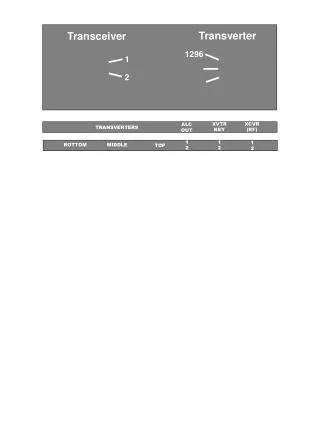
Equipment • Genesys FPGA board • Xilinx • Diligent PmodDA2 • Diligent PmodAD1 Figure 4: Genesys FPGA board
Specifications Figure 5: Specifications
FPGA System Clock = 100 MHz • Symbol Rate Rs = 12.5 Msps • Data rate Rb= Rs · N = 50 Mbps • Bits per symbol N = 4 • Symbol time = 1/ Rs
Stage 1 Simulink simulation • A single subcarrier carries data. Figure 6: 1 Frequency
Stage 1 Simulink simulation • Two subcarriers carry data. Figure 7: 2 frequencies
32 subcarriers Figure 8: 32 frequencies
Simulink Model • Model contains transmitter, receiver, and a Gaussian channel model. • Channel model • Y(t) = x(t)*h(t) • where x(t) is the transmitted signal, h(t) is the impulse response of the channel, and y(t) is the received signal.
Simulink results Figure 9: Input and Output from Transceiver
Stage 2: Implementation with channel effects • The transmitter and receiver are implemented on a FPGA board using VHDL. • Analog-to-digital converter (ADC) and digital-to-analog converter (DAC) modules are included. • Channel effects degrade the overall system performance.
Conclusion • In this project, a complete OFDM transceiver has been designed, simulated and tested. • First the simulink model of OFDM transceiver was constructed and simulated • After verifying the simulink model, VHDL is used to describe the transceiver • The system has been implemented on a Virtex 5 FPGA board. • 16 QAM is used for baseband modulation. Some modules from the previous project was reconfigured and used for the project
References • [1] Anthony Gaught, Alexander Norton, and Christopher Brady., “FPGA-based 16 QAM communication system”, Spring 2013. • [2]Leon Couch, Jr. “Analog and Digital Communication Systems”, 8th edition, 2012, Prentice-Hall.