Chapter 12. Digital Data Communications
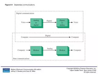
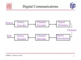
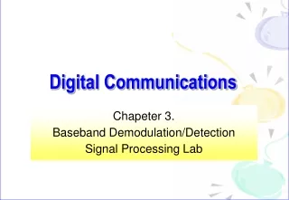
Chapter 12. Digital Data Communications. Figure 12-1. Binary transmission. Binary Data Transmission. Fig. 12-2. Four-level transmission of a binary message, at (a). the same transmission rate; (b). one-half the binary transmission rate. Bandwidth Considerations.

Chapter 12. Digital Data Communications
E N D
Presentation Transcript
Chapter 12. Digital Data Communications Figure 12-1. Binary transmission.
Binary Data Transmission Fig. 12-2. Four-level transmission of a binary message, at (a). the same transmission rate; (b). one-half the binary transmission rate.
Bandwidth Considerations • As seen in Figure 12-5, sharp digital pulses require a tremendous amount of frequency spectrum (bandwidth). • Since transmission channels have a limited bandwidth, the communication system designer needs to know (1) the minimum possible bandwidth required for a given pulse rate and (2) how pulses can be shaped to minimize the bandwidth and distortion of the data pulses.
Bandwidth Considerations Fig. 12-5. Time/frequency description of rectangular pulse train.
Pulse Shape for Minimizing Bandwidth and Pulse Distortion • Figure 12-9 shows pulses and the first “lobe,” and indicates how power is more concentrated for some pulse shapes as compared to others. • As an example, the raised-cosine pulse is seen to have a faster spectral rolloff than rectangular pulses. • Thus, for a channel with a bandwidth wide enough to include the first lobe, transmitting raised-cosine pulses will result in the reception of more power with less pulse distortion than for rectangular pulses.
Pulse Shape for Minimizing Bandwidth and Pulse Distortion Fig. 12-9. Frequency spectra for three different digital transmission signal formats.
Digital Transmission Formats • Some of the more common digital formats are illustrated in Figure 12-10. The NRZ signal is the same as the common TTL format, and NRZ-B is a bipolar version. • The advantage of the RZ formats gave the advantage of a zero dc component, assuming an equal number of 1s and 0s occur during a message. • The dc component is an important consideration in noisy systems because dc changes due to short bursts of continuous 1s or 0s will change the decision threshold and can result in more errors.
Digital Transmission Formats Figure 12-10. A few digital transmission formats.
Digital Transmission Formats • An additional advantage of bipolar over polar (on/off) formats is that, for the same S/N, polar requires twice the average power (four times the peak power) compared to bipolar. • The biphase (Bi-f)format uses a +/- squarewave cycle for a MARK and a -/+ for a SPACE. Each bit period contains one full cycle, thereby eliminating dc wander problems inherent in all the above signal formats. • A disadvantage of biphase, and RZ is the requirement for twice the bandwidth of NRZ and NRZ-B.
Digital Transmission Formats • The AMI format (Figure 12-10e), called bipolar with a 50% duty cycle by the telephone industry, is similar to RZ except that alternate 1s are inverted. • The dc component is less than for RZ, the minimum bandwidth is less than for RZ and biphase. • An additional advantage of AMI is that, by detecting violations of the alternate-one rule, transmission errors can be detected.
POWER in DIGITAL SIGNALS • For equal number of 1s and 0s during a message, the power can be averaged over the message period and the signal modeled as a continuous pulse stream. The generalized pulse stream is shown in Figure 12-11. • The normalized (R = 1W) average power is derived for a signal f(t) from (12-13a) where T is the period of integration. If v(t) is a periodic signal with period To, then (12-13b)
POWER in DIGITAL SIGNALS Figure 12-11. Pulse streams. (a). Rectangular pulses. (b). Rectangular pulses with t/T = 0.5 (square wave).
POWER in DIGITAL SIGNALS • If the rectangular pulses of amplitude V in Figure 12-11a start at t = 0, then V, 0 <t<t v(t) = { (12-14) 0, t <t<T. • and, from Equation (12-13b), (12-15) • from which P = (t/T)(V2/R) (12-16)
POWER in DIGITAL SIGNALS • Since the rms (effective value) of a periodic wave is found from P = (Vrms)2/R, it follows that the rms voltage for rectangular pulses is Vrms = (t/T)1/2V (12-17) because P = (Vrms)2/R = [(t/T)1/2V]2/R = (tV2)/(TR). • In the squarewave case of Figure 12-11b, t/T = 0.5, so that P = V2/2R (squarewave; that is, NRZ signals). • So the rms voltage for the unipolar squarewave is Vrms = V/√2 -- just as it is for sinusoids.
POWER in DIGITAL SIGNALS • EXAMPLE 12-2: • Compare the power of an NRZ squarewave to NRZ-bipolar (NRZ-B) where the peak-to-peak amplitudes are equal (in order for the two signals to have the same S/N when received over a noisy channel). Refer to Figure 12-12. • Solution: The power in an NRZ signal is PNRZ = V2/2R. For the NRZ-B signal, V V/2 and, since there are pulses in each half-period (instead of a large pulse followed by a zero amplitude pulse), PNRZ-B = 2(V/2)2/2R = V2/4R
POWER in DIGITAL SIGNALS Figure 12-12. Comparison of NRZ and NRZ-bipolar.
POWER in DIGITAL SIGNALS • It is seen that the on/off NRZ signal has twice the power of the NRZ-B signal. • The instantaneous (peak) power for NRZ is V2/R, whereas the peak power for NRZ-B is (V/2)2/R = V2/4R, for a 4:1 difference in peak power. • A final comment on these two important digital formats is that the dc power for rectangular RZ and NRZ signals is found from (tV/T)2/R, whereas for the bipolar signal it is zero.
PCM SYSTEM ANALYSIS • The PCM system consists of analog and digital source, concentrated into a few digital channels or multiplexed into a single digital stream for transmission between DCEs. • Figure 12-13 shows the transmit/multiplex part of a PCM system in which each channel of information is digitally encoded, multiplexed with other similarly coded channels, and then transmitted after a framing bit is added. • The analog voice signal is transformer-coupled and band-limited to < 4kHz by the LPF. • The telephone signal samples at fs > 2fA(max) = 8kHz. The samples must be held long enough to be encoded but short enough to multiplex the other 24 channels and one framing bit – all within 1/8000 = 125 ms.
PCM SYSTEM ANALYSIS Figure 12-13. Multiplexed PCM transmitter system.
Resolution and Dynamic Range • Dynamic range is the ratio of largest-to-smallest analog signal that can be transmitted. • The resolution, or quantization (step) size q, is the smallest analog input voltage change that can be distinguished by the A/D converter. • From the linear ADC transfer characteristic of Figure 12-15, it can be seen that q = Vmax/M = VFS/M, that is, q = VFS/2n where q = resolution (smallest analog voltage change that can be distinguished); n = number of bits in the digital code word; VFS = full-scale voltage range for the analog signal.
Resolution and Dynamic Range Figure 12-15. Linear ADC.
Resolution and Dynamic Range • The analog dynamic range capability of a PCM system Vmax/Vmin is the same as the ADC parameters VFS/q. • Since M = 2n = VFS/q, the dynamic range (DR) is expressed mathematically as DR = Vmax/Vmin = VFS/q = 2n (12-19) or, in decibels, DR (dB) = 20.log(Vmax/Vmin) (12-20)
Resolution and Dynamic Range • Note that 20.log2n = 20n.log2 = 6.02n, so we can write Equ. (12-20) into DR (dB) ≒ 6n • which means that there are approximately 6 dB/bit of dynamic range capability for a linearly encoded PCM system. • Table 12-2 summarizes resolution, dynamic range, and accuracy for up to 16 bits, • where accuracy is the system resolution in percent of full-scale, or the maximum possible accuracy of the demodulated analog signal.
Resolution and Dynamic Range Table 12-2. Linear ADC.
Quantization Noise • As seen in Figure 12-15b, a digitally encoded analog sample will have an exact-amplitude uncertainty of +q/2. • Demodulated PCM can be thought of as the analog input with quantization noise added. • The quantization noise voltage Vqn is sawtoothed with a peak value of q/2 and can be calculated from the average normalized power of Equ. (12-13b). • On a time basis over a period To of the quantization noise voltage waveform (Figure 12-15b), vq(t) = -(q/To)t, then (12-21a) (12-21b)
Quantization Noise • Hence, the effective voltage is from Vqn = √Nq, Vqn = q/2√3 (12-22) in volts rms. • The noise power will be Nq = q2/12R (12-23) for a linear ADC characteristic.
Signal-to-Quantization Noise Ratio • As seen in Figure 12-15, the maximum peak-to-peak sinusoid voltage will be equivalent to qM; that is, Vs(pk-pk) = qM and Vs(pk) = qM/2 volts peak. • The rms value is Vrms = Vs(pk)/√2 = qM/2√2 volts rms. (12-24) • The average power of a sinusoidal signal is S = Vrms2/R = q2M2/8R (12-25)
Signal-to-Quantization Noise Ratio • Combining Eqs. (12-23) and (12-25) yields the maximum signal-to-quantization noise for a sinusoid quantized into M levels, S/Nq = (q2M2/8R)/(q2/12R) = (3/2)M2 (12-26) • This is the maximum S/N for a linear ADC. • For analog input signals of voltage Vs that are less than the maximum, substitute S = Vs2(pk-pk) for q2M2 in Equ. (12-26).
Companding Linear qunatizing in PCM has two major drawbacks: • First, the uniform step size means that weak analog signals have a much poorer S/Nq than the strong signals. • Second,systems of wide dynamic range require many encoding bits and consequently wide system bandwidth. • A technique to improve S/Nq for weak signals is to decrease the step size q for weak signals and increase it for strong signals, as illustrated in Figure 12-16. • This nonlinear companding tends to equalize the S/Nq (or signal-to-digitizing distortion) over the expected range of analog amplitudes and requires rather complex digital hardware.
Companding Figure 12-16. Nonlinear step-size qunatizing.
Companding • Another technique to accomplish the same result is to use a linear encoder preceded by an analog voltage compressor, which also helps to prevent high-level signals from saturating the system. • After decoding, a complementary expander restores the original dynamic range. • A companding curve is sketched in Figure 12-17.
Companding Figure 12-17. Companding curve.
Companding • North America employs AT&T’s m-255 companding shape, known as the “m” law, whereas in Europe, the CCITT specifies the “A” law. • The North American “m” law has 16 linear segments, 8 for positive and 8 for negative voltages. There are 16 steps of equal size in each chord (the short linear segment). A simplified sketch is shown in Figure 12-18. • As a practical matter, companding laws are quite similar, and despite the complex circuitry, LSI codecs are companding with digital techniques and make provisions for the use of either law.
Companding Figure 12-18. sketch of m-255 transfer characteristic.
Companding EXAMPLE 12-4: • The 24-channel (D1) AT&T T1 PCM carrier telephone system band-limits input voice frequencies in each channel to 4 kHz. • The ratio of maximum-to-minimum voice level gives a dynamic range of 72dB. • Following the multiplexing of the 24 digitized voice signals, a framing bit is inserted to synchronize the system and to identify each channel’s data. • Reference to Figure 12-19 should aid in visualizing this analysis.
Companding Figure 12-19. 24-channel PCM T1 system with individual codec per-channel multiplexing.
Companding 1. The minimum sampling rate is fs>fA(max) = 2x4 kHz = 8000 samples/second. 2. The voice dynamic range for long (toll-grade) lines is 72 dB, so the ratio of maximum to minimum analog signal levels to be resolved is found from Equ. (12-20): 72 dB = 20.log(Vmax/Vmin), and by the definition of logarithms, Vmax/Vmin = 1072/20 = 103.6 =3981 = M. 3. The number of bits required to quantize 3981 equal levels (linear ADC) is, from M =2n, using Equ. (12-3b), n = 3.32.log3981 = 3.32(3.6) = 11.95 or 12 bits This is also determined as: 6 dB/bit requires 72 dB/(6 dB/bit) = 12 bits.
Companding • By compressing the voice signal, the m-255 companding codec provides the same dynamic range with 256 discrete levels using 8 bits. • Eight bits are nearly worldwide practice for digital voice transmission. • If only one channel (telephone conversation) is transmitted, the bit (and baud) rate would be 8000 samples/second x 8 bits/sample = 64 kbps. • Thus, a 4-kHz voice channel digitized to 8 bits would require an absolute minimum bandwidth of BW = (1/2)fb = 64-kbps/2-bits/cycle = 32 kHz.
Companding Figure 12-20. T1 PCM frame, 50% RZ polar format.
Companding 6. Twenty-four 8-bit samples plus one framing bit are multiplexed at 8000 frames/second. The T1 bit (and baud) rate is (24 channels x 8 bits/channel) + 1 framing bit = 193 bits/frame. 193 bits/frame x 8000 frames/s = 1.544 Mbps. • So the T1 line carries 1.544 Mbps, which requires a base-band bandwidth of at least BW = fb/2 = (1.544Mbps)/2 = 772 kHz. AT&T typically uses closer to 1.5MHz for T1 line bandwidth. • Figure 12-20 illustrates in a unipolar-RZ format the 8-bit samples for one 24-channel frame and the frame bit. • Notice that each frame takes 1/8000 sec = 125 ms and that each bit gets a slot of time equal to 125 ms/193 bits = 648 ns. • The transmission format used for a T1 line is AMI with a 50% duty cycle (not illustrated in Figure 12-20), consequently, each pulse is only 324 ns wide.
Companding 8. As indicated in Figure 12-20, during every 6th frame, the 8th bit (LSB) of each channel is borrowed by the mP-controlled CPU, allowing numerous loop supervision signals, including off-hook conditions, rotary-dial pulses, call charging information, and so forth. • The signaling rate can be determined as follows: 6 frames x 125 ms/frame = 750 ms for a signaling rate of 1/750 ms = 4/3 kbps. • During the 6th frame, the LSB is borrowed from each channel, resulting in more quantization distortion; but this only occurs 17% (≒ 1/6) of the time.
PCM Telephone Circuitry Digital-to-Analog Converters (DACs) • The receiving end of a PCM system accepts a digitally encoded serial data stream. Framing bits help to separate the encoded samples into their respective channels, • then the receive side of each codec clocks the encoded samples into a register for short-term storage (buffering) and serial-to-parallel conversion. • A DAC circuit will convert the parallel digital bits (d1-d4 in Figure 12-21) to an analog voltage equal to the original sample with some quantization error.
Digital-to-Analog Converters (DACs) Figure 12-21. Serial-to-parallel and digital-to- analog conversion.
Digital-to-Analog Converters (DACs) Binary-Weighed Resistor Converter • A binary-weighted resistor type DAC is illustrated in Figure 12-22a. Here, Q1-Q4 are MOS transistors used as switches activated by the parallel data word. • Each closed switch sets up an amount of current determined by the reference voltage and series resistance 2(n-i)R. • A high-gain IC is used in a current-summing op-amp configuration, and the currents from each of the high data bits are summed in feedback resistor Rf to produce an output voltage VA.
Binary-Weighed Resistor Converter Figure 12-22. Binary-weighted resistor D/A converter. (a). Weighted resistor DAC; (b). Weighted current source implementation of binary-weighted resistor DAC.
Binary-Weighed Resistor Converter • Figure 12-22b shows an LSI implementation of the weighted-resistor DAC. • The bipolar transistors are current sources for each weighted bit and are switched on or off by means of the control diodes connected to each emitter. • The base of each transistor remains biased to +1.2V, so that when an input bit is high, the transistor current source is on.
Digital-to-Analog Converters (DACs) R-2R Ladder-Type D/A Converter. • The DAC shown in Figure 12-23 maintains constant impedance level R at any node 1 through n and constant IR (except during switching transitions). • Note that each switch, actuated by a parallel-data input bit, is connected to ground or to “virtual ground”V-. Consequently IR = VR/R is a constant. • However, IR divides into 1/2n binary weighted currents at each node.
R-2R Ladder-Type D/A Converter Figure 12-23. R-2R ladder-type D/A converter circuit.
R-2R Ladder-Type D/A Converter • These binary weighted currents are either shunted to ground or summed into Iout to determine the output analog VA, depending on the digital word status of d1-d4. • That is, Iout = (VR/R).[dn/2 + dn-1/4 + dn-2/8 +… + d1/2n] (12-28) for the inverting op-amp, VA = Rf.Iout (12-29)
R-2R Ladder-Type D/A Converter • The advantages of the R-2R ladder DAC are that only two resistor values (laser-trimmed) are used. • Impedance levels are constant at all nodes for constant switching speed. • Except for IMSB, the weighted currents are determined by resistor ratios (rather than absolute resistor values) for improved temperature tracking.