Download
1 / 50
530 likes | 749 Views
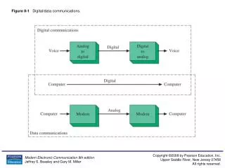
Figure 8-1 Digital/data communications. Figure 8-2 American Standard Code for Information Interchange (ASCII). Figure 8-3 The Extended Binary-Coded Decimal Interchange Code. Figure 8-4 The Baudot code. Figure 8-5 Baudot code examples. Figure 8-6 The Gray code.

E N D
Figure 8-2 American Standard Code for Information Interchange (ASCII).
Figure 8-3 The Extended Binary-Coded Decimal Interchange Code.
Figure 8-10 (continued) (a) Natural sampling; (b) flat-top sampling.
Figure 8-11 The sample frequency and input frequency relationship.
Figure 8-12 PCM encoding. (From the November 1972 issue of the Electronic Engineer, with the permission of the publisher.)
Figure 8-13 PCM TV transmission: (a) 5-bit resolution; (b) 8-bit resolution.
Figure 8-16 An example of 3-bit quantization with increased sample rate.
Figure 8-17 Uniform (left) and nonuniform (right) quantization.
Figure 8-27 Coding for a zero (00) and a one (11) for a minimum distance, Dmin, of 2.
Figure 8-28 A code message for a zero (000) and a one (111) with a minimum distance, Dmin, of 3.
Figure 8-29 ASCII code for A with odd parity. Note that lsb b1 is the first bit of the digital word transmitted.
Figure 8-33 CRC code generator for a (7, 4) cyclic code using a generator polynomial G(x) = x3 + x + 1.
Figure 8-34 A CRC divide circuit for the general form of G(x) = g0 + g1x + g2x2 + ··· + grxr.
Figure 8-36 (a), (b) Passive implementations for a second-order low-pass Butterworth filter and (c) a plot of the frequency response.
Figure 8-37 A second-order low-pass Butterworth active filter.
Figure 8-38 The block diagram for a digital signal processing circuit.
Figure 8-39 Input and output sequences for a second-order Iow-pass Butterworth filter at 3 frequencies: (a) 1000, (b) 2000 Hz, and (c) 500.
Figure 8-39 (continued) Input and output sequences for a second-order Iow-pass Butterworth filter at 3 frequencies: (a) 1000, (b) 2000 Hz, and (c) 500.
Figure 8-39 (continued) Input and output sequences for a second-order Iow-pass Butterworth filter at 3 frequencies: (a) 1000, (b) 2000 Hz, and (c) 500.
Figure 8-43 Effects of impedance mismatches: (a) impedance is too low; (b) impedance is too high (ringing); (c) impedance is matched.
Figure 8-44 Effects of frequency on data pulses: (a) good pulses; (b) low- frequency attenuation; (c) high-frequency attenuation.
Figure 8-45 A sample-and-hold circuit as implemented in Electronics WorkbenchTM Multisim.
Figure 8-46 The oscilloscope traces for the sample-and-hold circuit.
Figure 8-47 The spectrum of a signal that contains aliased frequencies due to improper selection of the sampling frequency.