Download
1 / 8
100 likes | 530 Views
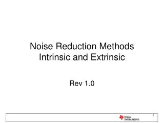
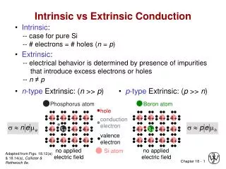
Intrinsic vs Extrinsic Conduction. 4. +. 4. +. 4. +. 4. +. 4. +. 4. +. 4. +. 4. +. 4. +. 4. +. 4. +. 4. +. 4. +. 4. +. • n -type Extrinsic: ( n >> p ). • p -type Extrinsic: ( p >> n ). 4. +. 4. +. 4. +. 4. +. 4. +. 4. +. 4. +. 4. +.

E N D
Intrinsic vs Extrinsic Conduction 4 + 4 + 4 + 4 + 4 + 4 + 4 + 4 + 4 + 4 + 4 + 4 + 4 + 4 + • n-type Extrinsic: (n >> p) • p-type Extrinsic: (p >> n) 4 + 4 + 4 + 4 + 4 + 4 + 4 + 4 + Phosphorus atom Boron atom hole conduction electron 5+ 3 + valence electron no applied no applied Si atom Adapted from Figs. 18.12(a) & 18.14(a), Callister & Rethwisch 8e. electric field electric field • Intrinsic: -- case for pure Si -- # electrons = # holes (n = p) • Extrinsic: -- electrical behavior is determined by presence of impurities that introduce excess electrons or holes -- n ≠ p
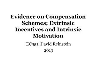
doped undoped 3 2 freeze-out extrinsic intrinsic concentration (1021/m3) Conduction electron 1 0 0 200 400 600 T (K) Adapted from Fig. 18.17, Callister & Rethwisch 8e. (Fig. 18.17 from S.M. Sze, Semiconductor Devices, Physics, and Technology, Bell Telephone Laboratories, Inc., 1985.) Extrinsic Semiconductors: Conductivity vs. Temperature • Data for Doped Silicon: -- s increases doping -- reason: imperfection sites lower the activation energy to produce mobile electrons. • Comparison:intrinsic vs extrinsic conduction... -- extrinsic doping level: 1021/m3 of a n-type donor impurity (such as P). -- for T < 100 K: "freeze-out“, thermal energy insufficient to excite electrons. -- for 150 K < T < 450 K: "extrinsic" -- for T >> 450 K: "intrinsic"
Hall Effect 18.41 A hypothetical metal is known to have an electrical resistivity of 4 10-8 (W-m). Through a specimen of this metal that is 25 mm thick is passed a current of 30 A; when a magnetic field of 0.75 tesla is simultaneously imposed in a direction perpendicular to that of the current, a Hall voltage of -1.26 10-7 V is measured. Compute (a) the electron mobility for this metal, and (b) the number of free electrons per cubic meter.
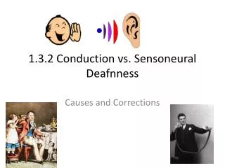
p-n Rectifying Junction + - + - + + - - + - p-type - n-type + + + - + - - + - - + n-type - p-type + + - - + + - + - + - • Allows flow of electrons in one direction only (e.g., useful to convert alternating current to direct current). • Processing: diffuse P into one side of a B-doped crystal. p-type n-type -- No applied potential: no net current flow. Adapted from Fig. 18.21 Callister & Rethwisch 8e. -- Forward bias: carriers flow through p-type and n-type regions; holes and electrons recombine at p-n junction; current flows. -- Reverse bias: carriers flow away from p-n junction; junction region depleted of carriers; little current flow.
Properties of Rectifying Junction Fig. 18.22, Callister & Rethwisch 8e. Fig. 18.23, Callister & Rethwisch 8e.
Junction Transistor Fig. 18.24, Callister & Rethwisch 8e.
MOSFET Transistor Integrated Circuit Device • Integrated circuits - state of the art ca. 50 nm line width • ~ 1,000,000,000 components on chip • chips formed one layer at a time Fig. 18.26, Callister & Rethwisch 8e. • MOSFET (metal oxide semiconductor field effect transistor)
Capacitance 18.51 Consider a parallel-plate capacitor having an area of 2500 mm2 and a plate separation of 2 mm, and with a material of dielectric constant 4.0 positioned between the plates. (a) What is the capacitance of this capacitor? (b) Compute the electric field that must be applied for 8.0 10-9 C to be stored on each plate.