Download
1 / 25
250 likes | 269 Views
This study examines the effects of hydrogen exposure on electron beam polarization from strained GaAs photocathodes. Motivations, experimental setup, tests performed, quantum efficiency, and polarization measurements from 2002 and 2003 are detailed. The research explores the changes in polarization, analyzing power, profilometry results, conclusions, and comparisons with other labs' methods.

E N D
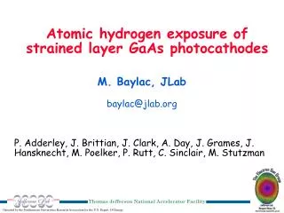
Effect of atomic hydrogen exposure on electron beam polarization from strained GaAs photocathodes M. Baylac, JLab baylac@jlab.org P. Adderley, J. Brittian, J. Clark, A. Day, J. Grames, J. Hansknecht, M. Poelker, M. Stutzman
Plan • Motivations • Experimental setup • Test • QE • Polarization measurements (2002 & 2003) • Analyzing power (2003) • Profilometry • Results, Conclusions
Motivations • Early days at JLab, wet chemical etching provided unreliable results: sometimes good, sometimes bad QE • Since 1995, atomic hydrogen cleaning provides high QE and reproducible results at JLab; other labs have adopted this method since then (MAMI, Nagoya, Bates, SLAC) • Polarization varied from wafer to wafer originating from the same manufacturer and across one single wafer (12 mm diameter) • What was JLab doing differently from SLAC? Study effect of hydrogen cleaning on wafer properties
split degeneracy of P 0.1 μm x=0.29 3/2 250 μm 250 μm p-type GaAs substrate GaAs GaAs P P x x 1-x 1-x 600 μm Strained layer GaAs photocathode Bandwidth Semiconductor (formerly SPIRE) Strained GaAs • MOCVD-grown epitaxial spin-polarizer wafer • Lattice mismatch 0<x<0.29
Photocathode preparation • 3” wafer cleaved (15.5 mm) • No wet chemical treatment, ie: no acid or base etching, no degreasing, no anodization • Sample on stalk w/ Indium Ta cup lucky
Test Plan • Stalk installed in gun vacuum chamber, chamber evacuated & bake (250 C) • Wafer heated 2 hours at ~ 570 C (estimated wafer temperature) • NEA activation (Cs+NF3) in gun chamber, QE scan of wafer • 100 keV beam : QE, polarization vs. wavelength and vs. wafer location • Break vacuum, remove wafer from gun • Load in portable hydrogen cleaning chamber, pump down • Expose wafer to atomic hydrogen
~ G Hydrogen source wafer ~300C • H2 dissociation via RF inductive discharge • Parameters adjusted then, wafer exposed • Dose measured with an “ion counter” at chamber bottom • Conditions kept identical for all cleanings 15 cm 100 MHz 20 W Mc.Alpine & Schildknecht, Proceeding of IRE, 1959 (2099) H2, or D2
Hydrogen cleanerhttp://www.jlab.org/accel/inj_group/h2/portable_H2.html
Test gun • 100 keV DC beam • Wavelength tunable Ti:Sapp • (750-850 nm) • 10 Hz helicity reversal • Mott polarimeter : P • Beam dump : QE lenses e correctors viewers
840 nm 2 3 y 5 4 1 x QE % ~ 13 mm Initial benchmark, untreated surface Syst. ~ 10% Stat. only M. Baylac et al, SPIN 2002, 15th International Spin Physics Symposium proceedings, 1073 (2003).
QE at band-gap vs. Hydrogen exposure At 840 nm Significant drop in QE vs. H cleaning Confirmed by 2 similar tests in different chamber w/o breaking vacuum
Polarization vs. cumulative H dose(central location) • Depolarization as H dose is increased • -dependent, strongest at band-gap • Found systematic effect: High H dose, QE low: ND filter removal increase non-IR light Depolarization due to low , high QE light Reject 60+ min. data
Depolarization tests • Confirm/infirm previous depolarization results • Test H+ ions effect • 3 independent tests, 3 photocathodes, only one change: • Usual exposure (no bias on photocathode during cleaning) • Ion-enhanced exposure (negative bias) • Ion-reduced exposure (positive bias) • Same method as before with one single exposure of 80 minutes for each test
Polarization with usual exposure P(H)-P(0)~-10% at bandgap 80 min dose
Polarization with ion-reduced exposure P(H)-P(0)~-10% at bandgap 80 min dose
Polarization with ion-enhanced exposure P(H)-P(0)~-20% at bandgap 80 min dose
Vacuum chamber GaAs x x x Cs NF3 x x i Insertable dissociator Insertable powermeter l/2 Analyzing power • Measure A.P. across strained-layer GaAs • 7 consecutive H exposures up to 4 hours 860 nm diode laser
Analyzing power (cont.) Analyzing power at 5 locations: ~ 5% and uniform
Analyzing power • No variation with H exposure, or location => Effect unrelated to strain
Profilometry after H exposure • A roughened surface could explain depolarization as effective angle of incidence of light onto wafer varies • High resolution 3d profilometry @ Jlab (Andy Wu) • area = 80 mm X 20 mm • vertical resolution = 7.4 Angstrom • Measurement of RMS roughness
Profilometry after H exposure Bare surface • RMS ~ 155 A H cleaned • RMS ~ 8500 A
Hydrogen exposure : results • Depolarization at band-gap induced by H exposure: confirmed at ~ 10% level systematics explains stronger effect seen on older data • QE seems to be only lowered by heavy H dose • Depolarization with/without H ions, unexplained enhancement • Increased anneal cycle (12 h instead of 2) does not restore Pe • Analyzing power independent of H • Surface analysis shows roughened surface which can explain depolarization (underway)