Download
1 / 28
300 likes | 573 Views
Xilinx CPLDs and FPGAs. Module M3. CPLDs and FPGAs. XC9500 CPLD XC4000 FPGA Spartan FPGA Spartan II FPGA Virtex FPGA. 3. In-System Programming Controller. JTAG Controller. JTAG Port. Function Block 1. I/O. I/O. Function Block 2. I/O. I/O Blocks. FastCONNECT Switch Matrix.

E N D
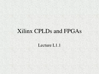
Xilinx CPLDs and FPGAs Module M3
CPLDs and FPGAs • XC9500 CPLD • XC4000 FPGA • Spartan FPGA • Spartan II FPGA • Virtex FPGA
3 In-System Programming Controller JTAG Controller JTAG Port Function Block1 I/O I/O Function Block 2 I/O I/O Blocks FastCONNECT Switch Matrix I/O Function Block 3 Global Clocks 3 Global Set/Reset 1 Function Block 4 Global Tri-States 2 or 4 XC9500 CPLDs • 5 volt in-system programmable (ISP) CPLDs • 5 ns pin-to-pin • 36 to 288 macrocells (6400 gates) • Industry’s best pin-locking architecture • 10,000 program/erase cycles • Complete IEEE 1149.1 JTAG capability
Global Clocks Global Tri-State 2 or 4 3 I/O Macrocell 1 Product- Term Allocator AND Array 36 From FastCONNECT I/O Macrocell 18 To FastCONNECT XC9500 Function Block Each function block is like a 36V18 !
XC9500 Product Family 9536 9572 95108 95144 95216 95288 Macrocells 36 72 108 144 216 288 Usable Gates 800 1600 2400 3200 4800 6400 tPD (ns) 5 7.5 7.5 7.5 10 10 Registers 36 72 108 144 216 288 Max I/O 34 72 108 133 166 192 VQ44 PC44 PC44 PC84 TQ100 PQ100 PC84 TQ100 PQ100 PQ160 PQ100 PQ160 Packages HQ208 BG352 PQ160 HQ208 BG352
CPLDs and FPGAs • XC9500 CPLD • XC4000 FPGA • Spartan FPGA • Spartan II FPGA • Virtex FPGA
XC4000 Architecture Programmable Interconnect I/O Blocks (IOBs) Configurable Logic Blocks (CLBs)
C2 C1 C3 C4 H1 DIN S/R EC S/R Control G4 DIN SD G G3 F' Q D Func. G' YQ G2 H' Gen. G1 EC RD 1 H G' Y Func. H' S/R Control Gen. F4 F F3 DIN SD Func. F' F2 Q D XQ Gen. G' F1 H' EC RD 1 H' X F' K XC4000E/X Configurable Logic Blocks • 2 Four-input function generators (Look Up Tables) - 16x1 RAM or Logic function • 2 Registers - Each can be configured as Flip Flop or Latch - Independent clock polarity - Synchronous and asynchronous Set/Reset
C2 C1 C3 C4 H1 DIN S/R EC S/R Control G4 DIN G G3 SD YQ F' Func. Q D G' G2 Gen. H' G1 EC RD 1 H Y G' H' Func. S/R Gen. Control F4 F F3 DIN Func. SD XQ F2 F' Gen. Q D G' F1 H' EC RD 1 X H' F' K XC4000 CLB
A B C D Z 0 0 0 0 0 0 0 0 1 0 0 0 1 0 0 0 0 1 1 1 0 1 0 0 1 0 1 0 1 1 . . . 1 1 0 0 0 1 1 0 1 0 1 1 1 0 0 1 1 1 1 1 Combinatorial Logic A B Z C D WE G4 G G3 Func. G2 Gen. G1 Look Up Tables Look Up Table • Combinatorial Logic is stored in 16x1 SRAM Look Up Tables (LUTs) in a CLB • Example: 4-bit address 4 (2 ) 2 = 64K ! • Capacity is limited by number of inputs, not complexity • Choose to use each function generator as 4 input logic (LUT) or as high speed sync.dual port RAM
XC4000X I/O Block Diagram Shaded areas are not included in XC4000E family.
CLB CLB Switch Matrix Switch Matrix CLB CLB Xilinx FPGA Routing • 1) Fast Direct Interconnect - CLB to CLB • 2) General Purpose Interconnect - Uses switch matrix • 3) Long Lines • Segmented across chip • Global clocks, lowest skew • 2 Tri-states per CLB for busses • Other routing types in CPLDs and XC6200
Other FPGA Resources • Tri-state buffers for busses (BUFT’s) • Global clock & high speed buffers (BUFG’s) • Wide Decoders (DECODEx) • Internal Oscillator (OSC4) • Global Reset to all Flip-Flops, Latches (STARTUP) • CLB special resources • Fast Carry logic built into CLBs • Synchronous Dual Port RAM • Boundary Scan
Programmable Interconnect Points, PIPs (White) Routed Wires (Blue) What’s Really In that Chip? Switch Matrix Direct Interconnect (Green) CLB (Red) Long Lines (Purple)
CPLDs and FPGAs • XC9500 CPLD • XC4000 FPGA • Spartan FPGA • Spartan II FPGA • Virtex FPGA
CPLDs and FPGAs • XC9500 CPLD • XC4000 FPGA • Spartan FPGA • Spartan II FPGA • Virtex FPGA
CPLDs and FPGAs • XC9500 CPLD • XC4000 FPGA • Spartan FPGA • Spartan II FPGA • Virtex FPGA