Pattern transfer by etching or lift-off processes
Pattern transfer by etching or lift-off processes. Basic pattern transfer steps. Positive resist (~1 m m thick) Film substrate. Hard mask. UV light. Glass opaque pattern. Film etching. Exposure. development. Resist stripping. Unexposed resist removed by resist striper.

Pattern transfer by etching or lift-off processes
E N D
Presentation Transcript
Basic pattern transfer steps Positive resist (~1mm thick) Film substrate Hard mask UV light Glass opaque pattern Film etching Exposure development Resist stripping Unexposed resist removed by resist striper - Exposed resist removed by developer - The resist pattern is the positive image of the pattern on the mask Resist protects the film areas
Pattern transfer by “lift-off “ lift-off etching - Allows use of hard-to-etch materials - Not for sub-micron features rounded top Wing tips
Requirements and constraints on lift-off Must avoid lateral step coverage • good edge definition depends on the lateral walls • avoid tearing or peeling of the remaining metal • easier to liftoff (solvent can reach the resist) Resist with slope or undercut profile: Create a descontinuity of the deposited film provides an area through which a solvent can pass to remove the resist resist resist substrate substrate • a) bake resist at 110ºC before exposure • (top surface becomes harder) • b) Double resist: resist I/resist II
Resist thickness > metal thickness For thick metal leyers: a) Increase the PR thickness b) Multiple layers: Resist/oxide Deposited film descontinuous resist resist substrate substrate Metal deposition temperature < ~250ºC (resist degradation) Some materials are deposited at high temperatures: - sputtered AlSiCu @400ºC “Burn” resist: ~100ºC (difficult to clean resist residues) Metal ductility determines success of liftoff • Britle materials: • tend to fracture at the edge of pattern steps (film discontinuity) • Ductile materials (e.g. Au): • poor edge definition or • impossible to liftoff
TiWN2 150 Å Ta 30 Å Ta 90 Å 100-250 Å MnIr NiFe NiFe 70 Å 70 Å Problems: fabrication of surface sensitivity devices Cannot deposit directly the device layers: The magnetic structure at the edges can be affected: The wafer surface was exposed to chemicals (vapor prime HMDS, resist, developer) resist 1.5 mm (15 000Å) 600 Å Magnetic tunnel junction
Isotropic or anisotropic selectivity overetch Pattern transfer by etching The resist and the substrate are also etched If the mask is etched too quickly: no control of the feature size To cope with film thickness and etch rate non-uniformities
Pattern transfer by etching Dry etching Wet etching
Wet etching SiO2 etching: SiO2 + 4 HF SiF4 + 2 H2O Al2O3 etching: Si etching: • Anisotropic etching of Si: atomically smooth planes and atomically sharp edges, at low cost
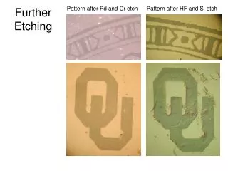
Defect-selective wet etching • Al2O3 etching • Oxide “pin-hole” detection Nucleation sites after wet etching Enhancement of local defects – can be counted in an optical microscope Si/NiFe 500Å/AlN 500Å
Dry etching Plasma + acceleration plasma