Download
1 / 47
470 likes | 490 Views
Explore latch flip-flops, synchronous systems, edge-triggered flip-flops, & more. Understand timing parameters & serial data transfers. Learn to troubleshoot, design oscillators, & use state transition diagrams. Incorporate PLDs & HDL code.

E N D
Chap. 5 Flip-Flops and Related Devices • Chapter Outcomes (Objectives) • Construct and analyze the operation of a latch flip-flop made from NAND or NOR gates. • Describe the difference between synchronous and asynchronous systems. • Describe the operation of edge-triggered flip-flops. • Analyze and apply the various flip-flop timing parameters specified by the manufacturers. • Explain the major differences between parallel and serial data transfers. • Draw the output timing waveforms of several types of flip-flops in response to a set of input signals. • Use state transition diagrams to describe counter operation. • Use flip-flops in synchronization circuits. • Connect shift registers as data transfer circuits. • Employ flip-flops as frequency-division and counting circuits. • Describe the typical characteristics of Schmitt triggers.
Chap. 5 Flip-Flops and Related Devices • Chapter Outcomes (Objectives) – cont. • Apply two different types of one-shots in circuit design. • Design a free-running oscillator using a 555 timer. • Recognize and predict the effects of clock skew on synchronous circuits. • Troubleshoot various types of flip-flop circuits. • Create sequential circuits with PLDs using schematic entry. • Write HDL code for latches. • Use logic primitives, components, and libraries in HDL code. • Build structural level circuits from components.
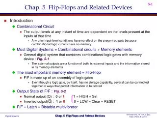
Chap. 5 Flip-Flops and Related Devices • Introduction • Combinational Circuit • The output levels at any instant of time are dependent on the levels present at the inputs at that time • Any prior input-level conditions have no effect on the present outputs because combinational logic circuits have no memory • Most Digital Systems =Combinational circuits+Memory elements • General digital system that combines combinational logic gates with memory device : Fig. 5-1 • The external outputs are a function of both its external inputs and the information stored in its memory elements • The most important memory element = Flip-Flop • F/F is made up of an assembly of logic gates : Feedback • Even though a logic gate, by itself, has no storage capability, several can be connected together in ways that permit information to be stored(Refer to Fig. 5-7). • Output State of F/F : Fig. 5-2 • Normal output (Q) : 0 or 1 1 = HIGH = Set • Inverted output(Q) : 1 or 0 0 = LOW = Clear = Reset • F/F = Latch = Bistable multivibrator (Refer to Slide 5-39). F/F : Clock Edge Sensitive Latch : Level Sensitive
1 1 0 1 1 1 1 0 1 1 Q 1 1 1 0 0 1 1 0 1 0 1 0 1 0 1 1 0 0 1 0 0 0 0 1 • 5-1 NAND Gate Latch • NAND gate latch(orLatch) • Constructed from two NAND gates : Fig. 5-3 • Setting the Latch • Both cases Q ends up HIGH : Fig. 5-4 • Clearing the Latch • Both cases Q ends up LOW : Fig. 5-5 • Simultaneous Setting and Clearing • Set = Clear = 0 • Q = = 1 : Undesired condition • Set = Clear = 1 • No change • NAND Latch Summary • Fig. 5-6(a),(b) Normally High Input Fig. 5-3 2 possible resting state when SET=RESET=1 Fig. 5-4 Pulsing SET input to 0 Fig. 5-3 참고 Normal rest 1 1 → Fig. 5-3 → Fig. 5-4 → Fig. 5-5 Fig. 5-5 Pulsing CLEAR input to 0
Q • Alternate Representations : Fig. 5-7 • Ex. 5-1)Determine Q output inFig. 5-8 • Ex. 5-2)Switch debouncing circuit inFig. 5-9 • 5-2 NOR gate Latch • Ex. 5-3) Determine Q output in Fig. 5-11 • Ex. 5-4) What happen if the light beam is momentarily interrupted in Fig. 5-12 • Q will remain HIGH and the alarm will remain ON even if phototransistor return to ON ( Set=0, Clear=0 : no change) • F/F State on Power-Up • When power is on, not possible to predict the starting state of a F/F’s output • Output depend on factors such as internal propagation delays, parasitic capacitance, and external loading. • To start of in a particular state, activate SET/CLEAR input at the start of circuit. Fig. 5-7 Alternate Representation 0 0 Resting Input = 0 * Invalid Q = = 0 0 1 Fig. 5-10 (a) NOR gate latch, (b) truth table, (c) simplified block symbol * Inactive Stage(Resting ) NAND latch : S=C=1 NOR latch : S=C=0 Ex. 5-4 SW1
5-3 Troubleshooting Case Study • Ex. 5-5) Describe & analyze the circuit in Fig. 5-13 • Ex. 5-6) What are the possible faults(refer to Tab. 5-1) • Possible faults(Switch position A에서 Fault : Q=1이여야 함) • Internal open at Z1-1 : 0이 입력되지 않음 SET=RESET=1 • Component failure in NAND gate Z1 • Internally shorted to ground at Z1-3, Z1-4, and Z2-2 • Node Q externally shorted to ground • 5-4 Digital Pulses • Pulse • A signal switches from a normal inactive state to the opposite (active) state, then the signal returns to its inactive state. • Positive pulse • Performs its intended function when it goes HIGH : Fig. 5-14(a) • Negative pulse • Performs its intended function when it goes LOW : Fig. 5-14(b) • Rise time tr / Fall time tf • The time it takes the voltage to change between 10% and 90% • Refer to Fig. 5-14(a), (b)
Fig. 5-13 : Example 5-5 0 1 0 0 1 0 0 1 1 0
Fig. 5-13 : Example 5-6 0 1 0 x 0 0 0 1 1
Leading edge • The transition at the beginning of the pulse • Trailing edge • The transition at the end of the pulse • Pulse width tw • The time between the points when the leading and trailing edges are at 50% • Ex. 5-7) Draw a scaled drawing of the RD pulse. : Fig. 5-15 • 5-5 Clock Signals and Clocked F/Fs • Async/Synchronous System • Asynchronous System : The output of logic circuits can change state any time • Synchronous System : The exact times at which any output can change states are determined by a signal commonly called the clock • Synchronous circuits are easier to design and troubleshoot because the circuit outputs can change only at specific instants of time. • Clock Signal = rectangular pulse train or square wave(Fig. 5-16) • Positive-Going Transition(PGT), Negative-Going Transition(NGT) • The synchronizing action of the clock signals is accomplished through the use of clocked flip-flops
0 1 0 0 0 0 1 1
Clocked Flip-Flops : Fig. 5-17 • 1. Clocked FFs have a clock input(CLK, CK, or CP) • In most clocked FFs, the CLK input is edge-triggered : NGT or PGT • 2. Clocked FFs have one or more control inputs • The control inputs will have no effect on Q until the active clock transition occurs(=Synchronous control inputs) • 3. In summary, • The control inputs control the WHAT : Output state(DATA 0 or 1) will go to • The clock input determines the WHEN : actually triggers the change • Setup and Hold Times : Fig. 5-18 • Setup time(5 - 50 ns) • minimum time that control input must remain at constant value before the transition. • Hold time(0 - 10 ns) • minimum time that control input must not change after the positive transition 50 % Fig. 5-18 Control Input Clock Input Positive clock transition ts th
4 possibleresults : Fig. 5-19 • a. the output does not respond at all to the HIGH : not change • b. the output tries to go HIGH but falls back LOW : meta-stable(settle LOW) • c. the output begins to go HIGH, waivers indecisively in the invalid region, and then responds appropriately by settling HIGH : meta-stable(settle HIGH) • d. the output responds as intended by going HIGH • 5-6 Clocked S-C F/F • Clocked S-C F/F • Waveform analysis in Fig. 5-20 : positive going edge transition Fig. 5-19 Set-Clear F/F
Q Q • The clock input = Trigger input • Negative-going edge transition : Fig. 5-21 • Internal circuitry of the edge-triggered S-C F/F • Edge-triggered S-C F/F : Fig. 5-22 • 1. NAND Latch • 2. Pulse-steering : NAND gate에 모두 1이 입력되면 SET/CLEAR= 0이 되고 Q=1/0 • 3. Edge-detector : Fig. 5-23 • 5-7 Clocked J-K F/F • Clocked J-K F/F : Fig. 5-24 • Toggle Mode : J = K = 1(S-C F/F에서는 Invalid) • Negative-going edge transition : Fig. 5-25 • Internal circuitry of the edge-triggered J-K F/F : Fig. 5-26 • Q=0, = 1인 상태에서 J=K=1이 입력되면 • NAND 1 의 입력은 모두 1이고 따라서 출력은 0이 되고 Q =1로 Toggle • NAND 2의 입력은 1, 1, 0이고 따라서 출력은 1이 되고 =0으로 Toggle • 5-8 Clocked D F/F • Clocked D F/F : Fig. 5-27 • Implementation of the D F/F : Fig. 5-28 • Parallel Data Transfer : Fig. 5-29 Jack-King F/F Data F/F
PGT NGT Fig. 5-23
1 1 0 1 1 2-5 ns Fig. 5-22 0 1 1 0 0 Fig. 5-22
1 0 1 0 → 1 0 x 1 1 1 1 1 1 → 0 1 0 Fig. 5-26
5-9D Latch : Transparent Latch • D Latch : Fig. 5-30 • Edge detector is not used : EN(Enable) input 사용 • Ex. 5-8) Determine waveform Q in Fig. 5-31 • 5-10Asynchronous Inputs • Asynchronous Inputs(= override inputs) • Used to set the FF to the 1 or clear the FF to the 0 state at any time, regardless of the conditions at the other inputs • Clocked J-K F/F with asynchronous inputs : Fig. 5-32 • Designations for Asynchronous Inputs • PRE(Preset), CLR(Clear) • SD(Direct SET), RD(Direct RESET) • Ex. 5-9) Determine the Q output in Fig. 5-33 D Latch is not Edge Triggered, (Level Triggered) Use the overbar to indicate the active LOW
1 1 0 1 1 1 1 0 1 0 Fig. 5-30
5-11 IEEE/ANSI Symbols : deleted in 11th Ed. • A single edge-triggered J-K flip-flop : Fig. 5-33(a) • 74LS112 dual edge-triggered J-K flip-flop : Fig. 5-33(b) • A single edge-triggered D flip-flop : Fig. 5-34(a) • 74HC175 quad D flip-flop common clock and clear : Fig. 5-34(b) • 5-11 F/F Timing Considerations • Setup/Hold Time : slide # 5-11 • Propagation Delays : Fig. 5-34 (Typ. MAX Few - 100 ns) • tPLH : Delay going from LOW to HIGH, tPHL : HIGH to LOW 50% CLK Fig. 5-34 Q tPLH tPHL
CLK • Maximum Clock Frequency :fMAX(Typ. Max 20 to 35 MHz) • Clock Pulse HIGH and LOW Times : Fig. 5-35(a) • The minimum time duration that the CLK must remain LOW before it goes HIGH tW(L), and HIGH before it returns LOW tW(H) • Asynchronous Active Pulse Width : Fig. 5-35(b) • The minimum time duration that a PRESET or CLEAR input must be kept in its active state in order to reliably set or clear the FF • tW(L) for active-LOW asynchronous inputs • Clock Transition Times • Manufacturer usually do not list a maximum transition time requirement • Generally less than 50 ns for TTL, and less than 200 ns for CMOS * removed in 12th ed. from here • Actual ICs : Tab. 5-2(TTL : 7474, 74LS112, CMOS : 74C74, 74HC112)
- 현재 그림은 정상 동작 - CLK 입력 전에 Q1 = 1 이며, CLK 입력과 동시에 J2 = 1이고 따라서 Q2 = 1 • 5-12Potential Timing Problem in FF Circuits • Potential Timing Problem : Fig. 5-36 • J2 input of Q2 will be changing as it receives the same NGT( ). This could lead to an unpredictable response at Q2 • 해결책 : Q1 tPHL must be greater than Q2’s hold time requirement • Hold time이 적다 = CLK 후에도 control input을 계속 유지시킬 필요 없음 • Fortunately, all modern edge-triggered FFs have hold time requirements that are 5 ns or less; most have tH = 0(clock transition과 동시에 control input이 바뀌어도 상관이 없다) • For these FFs, situation like that in Fig. 5-36 will not be a problem • 가정 : FF’s hold time requirement is short enough to respond reliably • The FF output will go to a state determined by the logic levels present at its synchronous control inputs just prior to the active clock transition • if we apply this rule to Fig. 5-35, J2 = 1, K2 = 0 • Ex. 5-10) Determine the Q output in Fig. 5-37 • Clock transition의 이전 입력 값을 갖는다 CLK 입력과 동시에 J2에는 1(Q1) 이 유지되어야 하지만 J1 = K1 = 1에 따라 Toggle되어 CLK 입력과 동시에 곧바로 J2 = 0이 되어 J2의 Hold time을 만족 시킬 수 없다
Q1 tPHL must be greater than Q2’s hold time requirement • 5-13FF Applications • Unclocked FFs • Switch debouncing(Ex. 5-2), Event storage(Ex. 5-4) • Clocked FFs • We will briefly introduce the more common applications in the following sections Fig. 5-36 Fig. 5-36
5-14FF Synchronization • Asynchronous signal input • A human operator’s actuating input switch at some random time • A FF can be used to synchronize the effect of an asynchronous input • Partial Pulse : Fig. 5-38 • The operator actuates or releases the switch are essentially random, This can produce partial clock pulses at output X • Ex. 5-11)A method for preventing the appearance of partial pulses : Fig. 5-39 • An edge-triggered D F/F is used to synchronize the enabling of the AND gate to the NGTs of the clock. • 5-15 Detecting an Input Sequence • Detecting an Input Sequence : Fig. 5-40 • An output is to be activated only when the inputs are activated in a certain sequence • HIGH output only if A goes HIGH and then B goes HIGH some time later • Ex. 5-12)A method for determining the direction of rotation : Fig. 5-41 • Use a D F/F to determine which direction the shaft is rotating • The D F/F detects this sequence FF Synchronization
5-16 Detecting a Transition or “Event” • The event detector for any given input signal : Fig. 5-42 • A data(binary • 5-17 Data Storage and Transfer • Register • A data(binary number, BCD number,..) are generally stored in groups of FFs called registers D CLK Q Fig. 5-41 D 1 1 0 0 Fig. 5-42 Q 0 1 1 0
Data Transfer • The data transfer involves the transfer of data from one FF or register to another • The logic value stored in FF A is transferred to FF B upon the NGT of the TRANSFER pulse • Synchronous data transfer : Fig. 5-43 • Asynchronous data transfer : Fig. 5-44 next slide • Transfer Enable = 0 : PRE=CLR=1, 통상적인 FF으로 동작 • Transfer Enable = 1 : A=1 이면 B=1, A=0 이면 B=0 • Parallel Data Transfer : Fig. 5-45 • The contents of X1, X2, and X3 are transferred simultaneously into Y1, Y2, and Y3(Upon application of the PGT of the TRANSFER pulse) • Parallel transfer does not change the contents of source register • 5-18 Serial Data Transfer : Shift Registers • Shift Register : Fig. 5-46 next slide • A group of FFs arranged so that the binary numbers stored in the FFs are shifted from one FF to the next for every clock pulse • Hold Time Requirement • In shift register, the FFs must have a very small or zero hold time requirement Sec. 5-12 Timing Problem과 동일
1 0 1 01 1 1 1 0 1 0 1 0 Enable 11 01 01 01 1 1 1 0 01 1 Disable0 Asynchronous data transfer : Fig. 5-44
01 11 1/0 • Serial Transfer between Registers : Fig. 5-47 • Ex. 5-13) The contents of each FF after sixth shift pulse in Fig. 5-47 ? • The registers are filled up with zeros(zero inserted) • Shift-Left Operation • 역으로 배치(Shift 방향에 따른 장단점은 없으며, 응용 특성에 따라 선택) • Parallel versus Serial Transfer • Parallel transfer : Speed • All of the information is transferred simultaneously upon the occurrence of a single transfer command pulse • Serial transfer : economy and simplicity • The complete transfer of N bits requires N clock pulses • 5-19 Frequency Division and Counting • 3 bit binary counter : Fig. 5-48 • The FFs change state(toggle) whenever the pulses are applied • Each FF divides the frequency of its input by 2 • Counting Operation : Fig. 5-49(State Table) • State Transition Diagram : Fig. 5-50 • Graphical representation of state table • Circle(state), Line(transition), I/O(input/output) 여러 개의 Transmission wire 필요 N 개 FF은 1/2N 까지 분주 가능 clock
MOD Number • MOD Number indicates the number of states • N Flip-flops = 2N different state, and count up to 2N - 1 • Ex. 5-14) What will be the state after 13 pulses(현재는 101) in Fig. 5-48 • Ex. 5-15) 6 Flip-flop arrangement of Fig. 5-48 • 5-20 Application of F/Fs with Timing Constraints • Counting up while it is rotating clockwise and then counting down when it is rotating counter-clockwise according to the physical position of the shaft • Problems using a simple sequence detector to create an absolute shaft encoder : Fig. 5-51 • t1 : the shaft encoder reversed its rotation, but did not count up because direction changes after clock • Block diagram of an absolute shaft position system : Fig. 5-52 • Edge detector in Fig. 5-42 : Enable control for Up/Down Counter • Direction decoder : Direction control for Up/Down Counter • Defining the direction decoder inputs [ DA, QA, DB, QB] : Fig. 5-53
Given Down 1 Up0 Up 4 not 2 Fig. 5-51
Fig. 5-52 Fig. 5-54 DA QA 1 4 t7 3 t4 1 3 2 2 4 4 2 2 3 1 3 4 1 DB QB Fig. 5-53 0 0 0 0 1 0 0 1 Given DA QA
Direction decoder truth table : Fig. 5-54 • 1. No change : disable [(0), (3), (12), (15)] : DA = QA and DB = QB • 2. Both change : impossible [(5), (6), (9), (10)] : DA = not QA and DB = not QB • 3. Direction 1(CW) : (2) = t4, (4) = t5/t1, (11) = t3, (13) = t2 • 4. Direction 0(CCW) : (1) = t7, (7)=t8, (8)=t10/t6, (14)=t9 • K-map, minimized Boolean equation, and logic circuit for the direction decoder : Fig. 5-55 • Timing Issues (Edge detect pulse width) : Fig. 5-56 • (a) up to one clock period wide : Fig. 5-56(a) • (b) very narrow and very close to the next PGT of clock : Fig. 5-56(b) Fig. 5-56
Improved quadrature encoder circuit : Fig. 5-57 • Adding synchronizing and data transfer FFs : Fig. 5-57(a) • Reliable operation depicted in a timing diagram : Fig. 5-57(b) A QSYNCH QXFER QEDGE DET EDGE-PULSE Setup time violation Fig. 5-57 0 1 1 1 0 0 0 1
STATE 1 0 VT- VT+ VOLT • 5-21 Microcomputer Application • Transfer binary data of internal register to external register X : Fig. 5-58 • 1) Place the binary number onto its data output lines • 2) Place the proper address code on its address output lines • 3) Generate the clock pulse CP(Write signal) • Ex. 5-16) a) What is address decode logic ? : 11111110 b) address code = 11111111일 때 X = ? : X will not change(그대로 0110) • 5-22Schmitt-Trigger Devices • Schmitt-Trigger Inverter : Fig. 5-59 • Schmitt-trigger type of input is designed to accept slow-change signals and produce an oscillation- free output 표시 : Fig. 5-59(b)
One-Shot tp • 5-23One-Shot (=Monostable Multivibrator) • One-Shot : Fig. 5-60(a) • 1) Once triggered by trigger input(T), Q = Opposite state • 2) “1” remains for a fixed period of time tp(Determined by tp = 0.69RC) • 3) After a time tp, the OS outputs return to their resting state(“0”) stable • Non-retriggerable One-Shot : Fig. 5-60(b) • Retriggerable One-Shot : Fig. 5-61 • Actual Devices : Fig. 5-62 • 74121/221 : • Single/Dual non-retriggerable one-shot • 74122/123 : • Single/Dual retriggerable one-shot Quasi-stable State 보통 “0” 에서 “1” Vcc * RINT : optional For output pulse width stability
5-24Clock Generator Circuits • Multivibrator • Bi-stable multivibrator : Flip-flops have two stable state • Mono-stable multivibrator : One-shots have one stable state(“0”) • Astable = Free-running multivibrator : no stable state • Schmitt-Trigger Oscillator : Fig. 5-63 • 555 Timer Used as an Astable Multivibrator : Fig. 5-64 • Ex. 5-17) Calculate the frequency and the duty cycle of the 555 timer • Ex. 5-18) Calculate RA and RB (less than 50%) • Crystal-Controlled Clock Generators • Output frequency = Crystal’s resonant frequency • Clock Generator Circuit : 10 kHz – 80 MHz • Using TTL inverter : R = 300 - 1500 Ohm, 최대 20 MHz • Using CMOS inverter : R = 100 K Ohm, 최대 10 MHz • 5-25 Troubleshooting FF circuits • Open Inputs : Ex. 5-19 ( Fig. 5-65 ) • K0가 Open 되어 J0 = K0 = 1 로 Toggle 됨(TTL open = 1) “1” = Quasi-Stable State * R depends on the type of crystal used and its frequency(Graph로 제공됨)
Q Q • Shorted Outputs : Ex. 5-20 ( Fig. 5-66 ) • D(Z2-2)에 0이 입력되며, 따라서 Q(Z2-5) = 0 이어야 정상 • Possible Circuit Faults • Z2-5 or Z1-4 is internally shorted to Vcc • Z2-5 or Z1-4 is externally shorted to Vcc • Z2-4 is internally or externally shorted to GROUND(Preset : Q = 1) • Z2 internal failure • In case of Z2 internal failure • 1) Check Z2’s Vcc and GROUND : O.K. • 2) Unsolder Z2, and Check it’s amplitude, frequency, pulse width, and transition times (by using oscilloscope) : O.K. • 3) Replace it with new one, but the new chip behaves in exactly the same way • 4) Finally he detects a solder bridge between pins 6 and 7 of Z2 • 5) Remove the solder bridge and then the circuit functions correctly • Explain how this fault produced the operation observed • The Q and outputs are internally cross-coupled so that the level on one will affect the other • A constant LOW at would keep a LOW at one input of NAND gate so that Q would have to stay HIGH regardless of the J or K 현재는 Q = 1 Rule out “1” “0” Both outputs should be checked for faults, even those that are not connected to other devices
01 1 0 1 1 1 0 1 Solder bridge Fig. 5-66
Clock Skew • A clock signal arrives at the CLK inputs of different FFs at different times(propagation delay가 원인) • The skew can cause a FF to go to a wrong state : Fig. 5-67 • Q2 는 CLOCK 1에서 Q1=0 이 입력되어 계속 Q2=0 이 되어야 함(그러나 그림에서는 CLOCK 2 이후에 Q2=1이 되어 오동작) • 해결 방법 • Problems caused by clock skew can be eliminated by equalizing the delays(the active transition arrives at each FF at approximately the same time) 각각의 Clock Input에서의 Propagation Delay를 계산
1 Fig. 5-67
5-26. Sequential Circuits in PLDs Using Schematic Entry * • Altera’s Quartus II development system software allows the designer the option of describing the desired circuit using schematics. • Quartus provides component libraries that contain flip-flop and latch devices that can be used to create the schematics. • These libraries are named primitives(dff, jkff..), maxplus2(macrofunction), and megafunction(LPM=Library of Parameterized Modules) • The megafunction library contains various high-level modules that can be used to create logic designs(LPM_FF, LPM_LATCH, and LPM_SHIFTREG..) • Exam. 5-21 : Compare the operation of a level-enabled D latch and edge-triggered D flip-flop • D latch and D flip-flop Quartus schematic: Fig. 5-68 • D latch and D flip-flop simulation report: Fig. 5-69
Exam. 5-22: Construct a register that consists of four D flip-flop using the D F/F primitive. • Input signals for Exam 5-22: Fig. 5-70 • Graphicconnection of D F/F primitives to form a 4 bit register: Fig. 5-71 • Schematic using a block symbol for a 4 bit D F/F register: Fig. 5-72 • Functional simulation results for Exam 5-22: Fig. 5-73 0 1 0 1 0 1 0 1
5-27. Sequential Circuits Using HDL • Three input/output modes : Fig. 5-74 • Behavioral description of an SR latch : Fig. 5-75 • Exam. 5-23 Describe S-R NAND latch (Fig. 5-6) • NAND latch using AHDL: Fig. 5-76 • NAND latch using VHDL : Fig. 5-77 • D latch : Fig. 5-30 • AHDL : variableqLATCH primitive (connection: q.ena=enable, q.d=din) • Tab. 5-2 Altera primitive port identifiers • VHDL : description (PROCESS) • 5-28. Edge-Triggered Devices • JK FF using AHDL : Fig. 5-78, Fig. 5-79 • standard JK FF is a fundamental part of sequential logic circuits called a logic primitive.- Tab. 5-2 • use logic primitives defined in library files to describe FF operation. • JK FF using VHDL • 1. Library component : Fig. 5-80 and Fig. 5-81 next slide • 2. explicitly describe logic circuit operation in the code : Fig. 5-82 1. Input only : D 2. Output only : Q 3. Output with feedback : Q VARIABLE ff1 :JKFF;
Library Components ( VHDL only ) • 1. Graphic representation using a component : Fig. 5-80(a) • Used again and again (exactly what IC manufacturers do) • VHDL component declaration : Fig. 5-80(b) • 2. JK FF component from the library in VHDL is used to create a circuit equivalent to the graphic design of Fig. 5-80(a) : Fig. 5-81 • Library define : ieee std logicandaltera components( VHDL only ) • Placing the following line at the top of your design file ( refer to Fig. 5-81). • Simulation of the JK FF : Fig. 5-83 • Verifying Fig. 5-79 (AHDL) and Fig. 5-82 (VHDL). • 5-29. HDL Circuits with Multiple Components • MOD-8 ripple counter / 3 bits Binary Counter : Fig. 5-84(=Fig. 5-48 ) • ADHL Ripple-up Counter : Fig. 5-85 • VHDL Ripple-up Counter : Fig. 5-86 No library is used, new neg_jk component define, describe explicitly LIBRARY ieee; define std_logic USE ieee.std_logic_1164.all LIBRARY altera; standard component USE altera.maxplus2.all