Download
1 / 68
680 likes | 731 Views
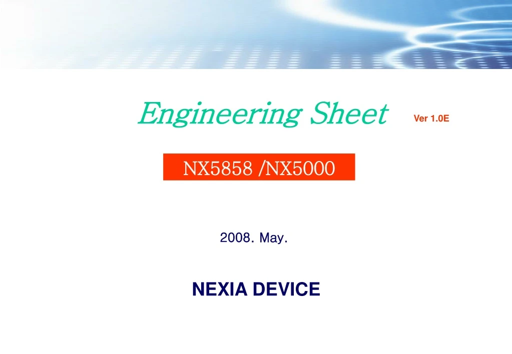
Engineering Sheet. Ver 1.0E. NX5858 /NX5000. 2008. May. NEXIA DEVICE. ■ INDEX. Ⅰ. General Features 1. Features -------------------------------------------- 3 2. Block Diagram ------------------------------------- 4 3. Processor ------------------------------------------- 5

E N D
EngineeringSheet Ver 1.0E NX5858 /NX5000 2008. May. NEXIA DEVICE
■ INDEX Ⅰ. General Features 1. Features -------------------------------------------- 3 2. Block Diagram ------------------------------------- 4 3.Processor ------------------------------------------- 5 4. Audio CODEC ------------------------------------- 6 5. Audio I/F & Effects ------------------------------- 7 6. Digital Amplifier ----------------------------------- 8 7. Video Decoding & LCD I/F -------------------- 9 8. DMA & I/F ----------------------------------------- 10 9. USB ------------------------------------------------- 11 10. Memory I/F --------------------------------------- 12 11. RTC & Analog Parts --------------------------- 13 Ⅱ. Pin Description 1. Pin Assignment ----------------------------------- 15 2. Pin Description ----------------------------------- 16 Ⅲ. Electrical Characteristics 1. Absolute maximum ratings -------------------- 24 2. Recommanded operating conditions -------- 25 3. DC Specifications -------------------------------- 26 4. Electrical characteristics for ADC ------------ 27 5. Electrical characteristics for PLL ------------- 28 6. Audio characteristics ---------------------------- 29 Ⅳ. Reference Schematics & Cautions 1. Schematic Block Diagram----------- 31 2. Schematic_MCU------------------ 32 3. Schematic_Reset------------------34 4. Schematic_Key ------------------- 35 5. Schematic_Flash Memory1 ---------- 36 6. Schematic_Flash Memory2 -------------------- 37 7. Schematic_Power_Charge --------------------- 38 8. Schematic_Power_PM1 ------------------------- 39 9. Schematic_Power_PM2 ------------------------- 40 10. Schematic_ Power_PM3 ------------------------ 41 11. Schematic_Audio1 -------------------------------- 42 12. Schematic_Audio2 -------------------------------- 43 13. Schematic_Audio_Mute ------------------------- 44 14. Schematic_LCD1 --------------------------------- 45 15. Schematic_LCD2 --------------------------------- 46 16. Schematic_USB ----------------------------------- 47 17. Schematic_FM ------------------------------------- 48 18. Schematic_Microphone ------------------------- 49 19. Schematic_Speaker ------------------------------ 50 20. Schematic_RTC ----------------------------------- 51 21. Schematic_Boot ----------------------------------- 52 Ⅴ. PCB Layout 1. PCB Component Layout ------------------------ 54 2. USB Pattern Layout ------------------------------ 55 3. D-Amp. Pattern Layout -------------------------- 56 4. FM Pattern Layout -------------------------------- 57 Ⅵ. Material Cost(M/C) 1. PCB Assembly M/C ---------------- 59 2. Total Cost ------------------------60 Ⅶ. PACKAGE 1. Package – TQFP ------------------ 62 2. Package – BGA ------------------- 63 1
2. Block Diagram Hardwired Multimedia Unit (Video Decoder/ MP3 Encoder/Decoder WMA/ASF Decoder) I/F (I2C,I2S,SPI, HPI,SPDIF) Hardwired Multimedia Unit (Video Decoder/ MP3 Encoder/Decoder WMA/ASF Decoder) Timer I/F (I2C,I2S,SPI, HPI,SPDIF) Timer DMA Controller DMA Controller • DISPLAY - OLED/LCD - JPEG/MJPEG - Graphical EQ H/W SRS-Wow HD BUS DRM Coprocessor H/W SRS-Wow HD DRM Coprocessor BUS H/W Graphical EQ(10 Band) • MP3 or MP3 with DRM • WMA with DRM • ASF H/W Graphical EQ(10 Band) USB 2.0 H.S Device USB 2.0 H.S Device SRAM SRAM(128K) UART USB 2.0 F.S Device GPIO Interface GPIO Interface D-Amp. for H/P (class-D) USB 2.0 F.S Device BUS BUS BUS BUS Digital Amp. BUS USB 1.1 Host BUS USB 1.1 Host UART USB 2.0(H.S)Device Memory Interface* Memory Interface* RISC I MCU RISC II MCU • Flash Memory - NAND/NOR/SD/MMC RISC I MCU RISC II MCU USB2.0 HS/FS USB1.1 Host • USB - USB2.0 HS/FS - USB1.1 Host USB 1.1 Host BUS BUS Boot ROM ADC PLL RTC LDO DC-DC Boot ROM PLL ADC RTC • Microphone • LINE_IN • FM_IN • Battery - AA/AAA - Li-ion 4
8. DMA & I/F 10
1. Pin Assignment * CASE 1 – TQFP type : 14X14 * CASE 2 – FBGA type : 8X8 NX5000 < Bottom View > < Top View > 15
3. DC Specification Note : 1. DVDD is ring DC supply voltage as stated in the operating conditions table. 26
4. Electrical Characteristics for ADC * Recommended Operating Conditions * Electrical Characteristics 27
6. Audio Characteristics * conditions: T = 25°C, VDD_core =1.3V, VDD_amp_power=2.7V, input sine wave with a frequency of 1kHz, EQ=off 29
Ⅳ. Reference Schematics & Cautions 30
1. Schematic Block Diagram * SYSTEM BLOCK Diagram FLASH MEMORY SD/MMC + FM C-MIC MIC-Amp. USB 2.0/1.1 PC MCU (NX5858) EarPhone 3.3V/2.7V/1.3V POWER (DC-DC/LDO) SPK-Amp. Speaker 8/16 bit Battery LCD (OLED/TFT/CSTN) KEY INPUT 31
2. Schematic _ MCU * CASE 1 - TQFP * Notice 1. Insert C-104 close to each Power Pins 2. Insert 12MHz Crystal closed to Pin and avoid analog signals. 3. Use 1%,F-grade Resistor(3.4K) for REXT(Pin No. 120) It’s important point 4. Separate each Ground 5. Insert components(C4,C5) for PLL close to each Pins 32
3. Schematic_Boot_Mode ■ BOOT_MODE select * Boot Mode Pin : 79, 80, 81 1) 80, 79(Boot_mode) pin - Boot mode ▶ If you use NAND Flash, connect 80(P11) to "high(33VD)" and connect 79(P10) to High/Low(Switchable) 2) 81(8/16bit mode) pin - 8bit or 16bit mode select - "H" : 16bit - "L“ : 8bit ▶ Generally connect to "GND" * Notice : At first, method to insert the F/W into the Flash Memory on boot mode 1. Making the special cable for inserting F/W (making 79 pin into “high” using spare pin of USB connector) 2. As above schematic, if you want normal mode then connect the pull-down resistor(47K) to 79pin. If you want “Boot mode” then add the pull-up resistor(1K) to 79 pin. After inserting F/W, you must delete the pull-up resistor. Then it’ll be changed to the normal mode. 33
3-1. Boot_Mode * CASE 1 * CASE 3 * CASE 2 * Boot Mode : It’s necessory to insert the program into the new flash memory. 1. It’s necessory for mass-product. 2. Case1 : Using pull-up and pull-down resistor. - Control the R1 resistor insert/delete. 3. Case2 : Using slide S/W - Control the slide-S/W up/down. 4. Case3 : Using Menu-S/W - Control the Menu key ON/OFF. If you press the menu button when you connect USB to PC, then you can download the F/W program. 34
4. Schematic _ RESET * CASE 1 * CASE 2 * CASE 3 * Notice 1. Hysteresis Curve about VDD Power_On time and Reset time (Chip_RST) is important 2. We recommand “Case 1” above 3 Cases 3. It’s better “Case 2” then “Case 3” on the cheep model. In case of “Case 3” is needed more Reset Test. 35
5. Schematic _ Key * Functions - PLAY(P-UP) / MENU / FF(▶) / REW(◀) / VOL_UP / VOL_DOWN * CASE 1 : Using GPIO Input Port * CASE 2 : Using ADC Port * Notice 1. If you have enough GPIO ports, it’s better using GPIO input port. 2. When use ADC Port(Case 2),Play key resistor’s value(R57) is mixed with Diode resistor’s value(D7). So notice the variation of resistor value between high and low temperature. 36
6. Schematic _ Flash Memory 1 1) NAND FLASH 2) SD/MMC * Notice 1. When you need 2 flash memory, you have to use another 2 CEs (FCE2, FCE3). 2. “/WP” is needed PULL-UP resistor and it’s allowed to control with MCU port. When “/WP” is “low”, then that status is disable to write. 3. You can extend Flash memory’s capacity using external memory(SD/MMC Card) 37
6. Schematic _ Flash Memory 2 3) NOR FLASH * Notice 1. Host products using SD/MMC Memory (if isn’t internal memory) need “Nor Flash” for program storage. 2. If you use “Nand Flash” memory, it doesn’t need “Nor Flash” memory. 38
7. Schematic _ Power_ Charge 5-1. Charger Part * CASE 2 : Cheep model - w/o Charge IC * CASE 1 : General - with Charge IC * CASE 3 : Cheep model - w/o Charge IC - MCU control USB-P * Notice 1. Charge the rechargeable battery with 4.2V from USB-Power, you can choose the suitable charge IC. 2. It’s safe to use the Charge-IC such as “Case 1”. It’s out signal from charge IC when is charged fully. 3. In case of cheep model, you can charge with 4.2V using zener-diode such as “Case 2”. But we don’t recommand it. 4. In case of “Case 3”, you can control the USB_Power supply by MCU port. When some time(3~5 hours) passed, it switch off(Q6). 39
7. Schematic _ Power _PM 1 5-2. DC-DC/LDO Part 1) Power 3.3V(LDO) for I/O 2) Power 2.7V (LDO) for D-Amp. * Notice 1. You can use 2.7V ~ 3.3V for I/O voltage. We recommand 3.0V. 2. It’s the normal method to use LDO for making power voltage from battery. It’s cheaper than DC/DC converter. But DC/DC converter is more efficient. If you want to play mp3 player more time, we recommand DC/DC converter. 3. You should use 2.7V ~ 3.3V LDO separated from other power voltage for D-amp. Power(pin no. 89/94) If you shouldn’t use it, it occurs noise. 40
7. Schematic _ Power _PM 2 3) 1.3V for Core Voltage 3-1) Using LDO 3-2) Using DC/DC Converter * Notice 1. Generally you can use 1.1V~1.4V for Core voltage. But we recommand 1.3V for it because it has better characteristics on data download with USB. 2. It’s better to use DC/DC converter then LDO for battery life. It will be save 2~3mA. But it’s cheaper LDO then DC/DC converter. 41
7. Schematic _ Power _PM 3 4) Power Control * Notice 1. When you press the PLAY button at Power_off status, ON/OFF signal will be “High” so it’ll be turned on. At the same time, Q5 is activated, then MCU recognize the “Play Key” is pressed. 2. Diode(D11)을 거쳐 POWER_EN에 “high”가 인가되어 LDO(U9)가 enable되어 전압이 인가된다. 3, 이때 MCU(NX5858)가 동작되어 P32/PWR이 “high”로 올라온다. 계속 “high”로 유지하고있기 때문에 Power-On중에는 계속 전원이 인가된다. 4. Power-On중에 Play Key를 길게 누르면 Power-off mode로 MCU가 인식하게 되고 이때 P32/PWR port를 “low”로 내리게 되어 PWR_EN이 “low”로 되어 LDO가 off되게된다. 5. USB에 연결시 무조건 USB_P가 인가되어 PWR_EN이 무조건 “high”가 되어 LDO가 ON 된다. * Notice 1. Power_off 상태에서 Play Key를 누르면 ON/OFF에 “high”가 인가됨. Play Key를 누를때마다 Q5가 도통되어 P17/PLY port가 “low”로 떨어지게되어 Play Key를 인식하게 된다. 2. Diode(D11)을 거쳐 POWER_EN에 “high”가 인가되어 LDO(U9)가 enable되어 전압이 인가된다. 3, 이때 MCU(NX5858)가 동작되어 P32/PWR이 “high”로 올라온다. 계속 “high”로 유지하고있기 때문에 Power-On중에는 계속 전원이 인가된다. 4. Power-On중에 Play Key를 길게 누르면 Power-off mode로 MCU가 인식하게 되고 이때 P32/PWR port를 “low”로 내리게 되어 PWR_EN이 “low”로 되어 LDO가 off되게된다. 5. USB에 연결시 무조건 USB_P가 인가되어 PWR_EN이 무조건 “high”가 되어 LDO가 ON 된다. 42
8. Schematic _ Audio 1 * CASE 1 – Digital Amp. 사용 * Caution 1. D-Amp.의 전원은 반드시 별도의 LDO로 분리하여 사용하도록 한다. 아니면 White Noise가 심할수 있다. 2. AMP_L/R 출력은 PWM 파형으로서 EMI의 Source가 되기도 한다. Port AMP_L/R에서 Coil (HL2,3) 사이는 PWM 의 강력한 AC성분으로 주변 signal에 영향을 미칠수 있다. 오디오 signal은 피하고 pattern은 최대한 짧게한다. 3. 2차 필터인 HL2,3와 HC1,2는 다음의 범위에서 알맞게 정한다. Cutoff 주파수가 40~80kHz가 되도록 설계한다. 20uH<HL<80uH, 0.1uF<HC<0.47uF (가능한한 L값을 크게해야 ripple current가 줄어든다.) ex1) HL=82uH, HC=104 / ex2) HL=22uH, HC=474 4. AC Coupling Cap.인 HCE1,2는 220uF가 정상이나 100uF도 가능하다. 5. Pop-up Noise를 없애기위하여 Mute단(Q3,4)을 구성하여 필요시 Muting처리한다. 6. D-amp.의 특성상 Low-frequency에서의 특성이 안좋을 수 있다. 주의 한다. 43
8. Schematic _ Audio 2 * CASE 2 – 외부 Audio CODEC(WM8750L) 사용 * Notice 1. I2S 통신을 사용하여 외부 CODEC으로 Encoding과 Decoding을 할 수 있다. NX 5858 내부 ADC를 이용시 10bit이므로 품질을 만족 못할시 외부 CODEC을 사용한다. 2. 외부 CODEC 선정시 회사에따라 전류소모가 차이가 많이 나므로 선정하는데 주의한다. 전류소모 기준으로 Wolfson사의 WM8750L/8731L/8711L(DAC)등 뒤에 “L”이 붙는 모델이 저전력용이다. WM8750L은 Speaker Amp.까지 내장되어 있다. 44
8. Schematic _ Audio_Mute * Audio Mute 적용 * Notice 1. Power-On시 또는 기타 불필요한 음이 들리는걸 막아주기위한 기본 대처로 Mute단을 설계하여 적용한다. 2. TR.을 사용하여(L, R 각각) Mute on시 Audio Signal을 GND로 muting한다. 3. Mute signal이 “high” 일 때 Mute “On” 이다. Mute는 재생시에만 Off하며 기타는 On 상태를 유지한다. Play Key입력시 data output하고 이어서 Mute를 off해야 불필요한 pop-noise를 막을수 있다. Stop시는 반대로 Mute on 먼저하고 이어서 data를 off한다. 4. Sirial 저항 MR11,12의 저항값이 높을 수록 Muting의 효과가 크다. 하지만 이 저항이 크면 반비례하여 출력이 떨어진다.(출력 Level 감소) 5. MR13,14는 출력단의 충전 time을 조절하는 저항이며(Aux. Charging Resister) 2.2K를 기본으로한다. Pop noise가 발생시 이부분의 저항을 줄이면 약간의 효과를 볼 수 도 있다. 45
9. Schematic _ LCD 1 * CASE 1 – TFT LCD (320 X 240) 사용 * Notice 1. Display는 320x240까지 사용할 수 있으며 그 이상은 performance상 힘들다. 2. 가로 size는 16의 배수, 세로 size는 8의 배수가 되어야 한다. 3. LCD와 interface는 8/16bit둘다 가능하다. 4. Bacllight LED를 위한 step-up DC/DC Converter 를 별도로 사용하여 전원(약 11V~13V)을 공급 해줘야 한다. 5. TFT-LCD, OLED, CSTN 등 대부분의 적용이 가능하다. 46
9. Schematic _ LCD 2 * CASE 2 – OLED(128 X 128) 사용 47
10. Schematic _ USB * CASE 1 * Notice 1. USB Jack의 D+, D- Pattern은 NX5858 pin에 최대한 가깝게, 굽어짐이 없이streight로 연결되어야 한다. 피치 못하게 굽어져서 연결될때는 최소화하고 angle을 줘서 직각이 되지 않도록 한다. 중간에 어떠한 저항이나 콘덴서도 연결되지 않도록 한다. 2. NX5858의 120번Pin REXT 저항은 반드시 3.4Kohm, F급(허용오차 1%)을 사용하여야 한다. 3. USB_ detector(UDET)는 USB 전원(USB_P)을 devide하여 2.0V~3.0V 사이가 되게 한다. 48
11. Schematic _ FM * CASE 1 – FM Module 사용 * Notice 1. I2C 통신을 사용하여 외부 FM chip 또는 Module과 interface하여 control할 수 있다. 2. Antenna는 earphone의 GND를 이용하며 Coil로 분리하여 DC적으로는 short, AC적으로는 분리한다. FM Module의 Antenna와 이어폰의 GND(FM_ANT)는 최대한 가까운게 유리하다. Pattern 연결시 주변에 영향을주는 signal을 피해서 연결한다. 전체적인 임디던스에 맞는 인덕터(Coil)를 선정하여 실장한다. 3. FR9,10과 FC7,8이 없으면 간헐 통신시 FM에 노이즈가 유기하기도 한다. 4. FM 출력을 ADC2,4의 ADC input으로 넣어준다. 외부 CODEC사용시 외부 CODEC input port로 넣어준다. 내부 ADC이용시 10bit이므로 음질이 다소 나빠질수 있다. 고품질을 원할시 외부 CODEC을 사용한다. 49