Download
1 / 20
1.21k likes | 4.21k Views
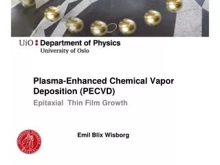
Plasma-Enhanced Chemical Vapor Deposition (PECVD). Epitaxial Thin Film Growth Emil Blix Wisborg. What is CVD?. Chemical Vapor Deposition Deposition of a solid phase from a gaseous phase Volatile precursor gases react or decompose on a heated substrate

E N D
Plasma-Enhanced Chemical Vapor Deposition (PECVD) Epitaxial Thin Film Growth Emil Blix Wisborg
What is CVD? • Chemical Vapor Deposition • Deposition of a solid phase from a gaseous phase • Volatile precursor gases react or decompose on a heated substrate • Operating temperatures 400-1200°C
CVD process example • Gas-phase decomposition • Diffusion to surface • Physical adsorption • Diffusion along surface • Decomposition • Desorption of reaction by-products S. A. Campbell, Fabrication Engineering at the Micro- and Nanoscale, 4th Ed., Oxford UniversityPress (2013)
Thin films • A layer of material ranging from a few Ångstrøms to several microns • Electronic semiconductor devices • Solar cells • Batteries • Optical coatings • Mirrors • Antireflection coating
Epitaxy • Depositionof a crystallineoverlayeron a crystallinesubstrate • Continouscrystalstructure • Homoepitaxy • Film and substrate same material • Highpuritylayers and doping control • Heteroepitaxy • Film and substratedifferent material • Bandgapengineering
Epitaxy GaN→ AlGaN→ AlGaN→ AlN→ GaN→ GaN→ GaN→ GaN→ Dr. Alan Doolittle, Georgia Tech, ECE6450: CVD and Epitaxy
What is PECVD? • Plasma-enhanced CVD • Energy required for reactioncomes from plasma ratherthan from temperature • Waferscan be kept at lowtemperature • The plasma is created by RF electromagneticwaves
PECVD theory – plasma • Fractionally ionized gas • High free electron content • Two main types: • Hot (thermal) plasma • kT > Eionization • Thermalequilibrium, Te≈Tgas • Cold plasma • Createdby electricfieldsor radiation • Non-thermalequilibrium, Te>>Tgas
PECVD theory – sheath • The plasma forms a thinpotentialdrop at all surfaces - sheath • Causes an electricfield from the plasma to thesurface • IfE = 0: • Particle-surfacecollision rate: n v • v ~ √{T/m} • velectron > vion • Drainofelectrons from plasma I.H.Hutchinson: Introduction to Plasma Physics, http://silas.psfc.mit.edu/introplasma/chap1.html
PECVD theory – sheath • The plasma forms a thinpotentialdrop at all surfaces - sheath • Causes an electricfield from the plasma to thesurface • Plasma becomespositivelycharged • Positivelychargedparticlesareacceleratedtowardthesurface E I.H.Hutchinson: Introduction to Plasma Physics, http://silas.psfc.mit.edu/introplasma/chap1.html
Process steps • Precursor gas and carrier gas mixed in reaction chamber • Ionization to plasma by RF electric field • Energetic electrons dissociate precursor molecules to free radicals • Particles move to substrate • Radicals adsorbed onto substrate (and reactor walls) • Layer formation • Density increased by ion bombardment A. Barron, ‘ChemicalVaporDeposition’ , Connexions Web site, Mar 12, 2014.http://cnx.org/content/m25495/1.2/
Reactors • S. A. Campbell, FabricationEngineering at the Micro- and Nanoscale, 4th Ed., Oxford University Press (2013) Hot wall Cold wall
PECVD trends (SiH4basedprocesses) Oxford Instruments, Plasma Technology. http://www.ndl.org.tw/cht/doc/3-1-1-0/T19/T19_B1.pdf
Advantages of using PECVD • Low operating temperature • Uniform coating of different shapes Conformal step coverage of PECVD SixNy Royal Philips Electronics, http://www.hitech-projects.com/dts/docs/pecvd.htm
Advantages of using PECVD • Low operating temperature • Uniform coating of different shapes • Good step coverage • High packing density – hard and environmentally stable • Continuous variation of film characteristics as a function of depth • Stress reduction
Drawbacks • Toxic precursors and byproducts • High equipment cost • Limited capacity • Contamination from precursor and carrier gas molecules • Silane (SiH4) often used as Si source • Hard to obtain stoichiometry • Silicon nitride (SixNy) and silicon oxide (SiOx)
PECVD at UiO • Advanced Vacuum Vision 310 MKII • Located in the cleanroom • SiO2 • Si3N4 • SiON • a-Si • Up to 12” wafer size • No polymers or organic materials
References • Wikipedia: ‘Plasma-enhanced chemical vapor deposition’. http://en.wikipedia.org/wiki/Plasma-enhanced_chemical_vapor_deposition • http://www.oxford-instruments.com/products/etching-deposition-and-growth/plasma-etch-deposition/pecvd • S. A. Campbell, Fabrication Engineering at the Micro- and Nanoscale, 4th Ed., Oxford UniversityPress (2013) • A. Barron, ‘ChemicalVaporDeposition’ , Connexions Web site.http://cnx.org/content/m25495/1.2/ • T. Finstad, FYS4310: Materials Science of Semiconductors • TimeDomain CVD Inc., ‘Capacitive Plasmas’ http://timedomaincvd.com/CVD_Fundamentals/plasmas/capacitive_plasma.html • Wikipedia: ‘Thin film’. http://en.wikipedia.org/wiki/Thin_film • Jung-Hyun Park: Deposition of Coatings by PECVD. http://www.docstoc.com/docs/59194062/Deposition-of-Coatings-by-PECVD All websites accessed latest at March 12, 2014
Questions? Thank you for your attention!