Download
1 / 37
370 likes | 583 Views
EET 1131 Unit 14 Memory and Storage. Read Kleitz , Chapter 16. Lab #14 due next week. Final Exam next week. Terms for Units of Data. Bit : The smallest unit of digital data, a single 1 or 0. Byte : A group of 8 bits. Nibble : A “half-byte”: a group of 4 bits. Word : Used in two ways:

E N D
EET 1131 Unit 14Memory and Storage • Read Kleitz, Chapter 16. • Lab #14 due next week. • Final Exam next week.
Terms for Units of Data • Bit: The smallest unit of digital data, a single 1 or 0. • Byte: A group of 8 bits. • Nibble: A “half-byte”: a group of 4 bits. • Word: Used in two ways: • Sometimes means 2 bytes (or 16 bits). • Sometimes means the data width that a particular chip or system uses: could be 4 bits, 8 bits, 16 bits, 32 bits, etc.
Kilo-, Mega-, Giga- • In engineering notation, • Kilo means 1,000 (the same as 103) • Mega means 1,000,000 (same as 106) • Giga means 1,000,000,000 (same as 109) • When talking about memories, these terms have slightly different meanings: • Kilo means 1,024 (the same as 210) • Mega means 1,048,576 (same as 220) • Giga means 1,073,741,824 (same as 230)
Making Sense of Windows File Sizes • Have you ever noticed that when you use Windows to look at a file’s size, it gives two numbers that don’t seem to match each other? • Example:“Size on disk: 624 KB (638,976 bytes)” • That’s because 624 x 1024 = 638,976. • How many megabytes (MB) is in a file that contains 28,311,552 bytes?
Memory Units The location of a unit of data in a memory is called the address. In personal computer memories, a byte is the smallest unit of data that can be addressed. For example the blue byte is located in address 6.
Computer Busses • A computer system has two primary busses: • The data bus, which carries data and instructions from one part of the system to another. • The address bus, which carries addresses of memory locations or external devices. • These two busses may have the same width (number of bits), but they need not. • When people talk about a “16-bit system” or a “32-bit system,” they’re talking about the width of the data bus.
Write Operations The two main memory operations are called read and write. A simplified write operation is shown in which new data overwrites the original data. Data moves to the memory. Address register Data register Address decoder Byte organized memory array Address bus • The address is placed on the address bus. • Data is placed on the data bus. • A write command is issued. Data bus Write
Read Operations The read operation is actually a “copy” operation, as the original data is not changed. The data bus is a “two-way” path; data moves from the memory during a read operation. Address register Data register Address decoder Byte organized memory array Address bus Data bus • The address is placed on the address bus. • A read command is issued. • A copy of the data is placed in the data bus and shifted into the data register. Read
Some Common Address Bus Widths • An address bus’s width (in bits) determines the number of locations it can address:
Powers of 2 • Here’s a handy table showing the powers of 2 up to 240. • You can use a table like this to answer the following questions: • How many addressable locations are there in a memory with n address bits? • How many rows are there in a truth table with n input variables? • What is the MOD of an n-bit counter?
Designating a Memory Chip’s Size & Layout • The size and organization of a memory chip is given by a designation such as 16 x 4. • The first number (16 in our example) tells how many addressable locations the chip contains. • The second number (4 in our example) tells how many bits are contained in each of these addressable locations. • Thus, an 8 x 8 chip, a 16 x 4 chip, and a 64 x 1 chip all have a bit capacity of 64 bits, but they’re organized differently.
Address Input Pins • We can tell how many address pins a memory chip needs by looking at the first number in its designation. • For example, a 16 x 4 chip has 16 addressable locations. How many address pins are needed if we want to be able to select any one of these 16 locations? • How many address pins would an 8 x 8 chip need? • How many address pins would a 64 x 1 chip need?
Data Output Pins • We can tell how many data output pins a memory chip needs by looking at the second number in its designation. • For example, on a 16 x 4 chip, each location contains 4 bits, so to read out the contents of any location, we need 4 data output pins. • How many data output pins would an 8 x 8 chip need? • How many data output pins would a 64 x 1 chip need?
Data Input Pins? • Some memory chips are read-only memories (ROMs). These chips don’t have data input pins because you cannot change the contents of the memory locations. • Other memory chips are read-write memories (confusingly called RAMs, for “random-access memory”). These may have data input pins that are separate from the data output pins, or the pins may be combined as data input/output (I/O) pins.
Some Memory Chip Datasheets • 7489 RAM (16 x 4) • 6116 RAM (2048 x 8) • TMS4700 ROM (1024 x 8)
Chip Select (CS) or Chip Enable (CE) is used as part of address decoding. All other inputs are ignored if the Chip Select is not active. ReadEnable (RE) and WriteEnable (WE) signals are sent from the CPU to memory to control data transfer to or from memory. Output Enable (OE) is active during a read operation, otherwise it is inactive. It connects the memory to the data bus. Memory Addressing In addition to the address bus and data bus, semiconductor memories have read and write control signals and chip select signals. Depending on the type of memory, other signals may be required.
Computer Memory • A computer’s memory consists of many memory chips, which may be organized in different ways. • Example: in the tiny memory below, each byte may be contained on a single chip, or may be spread across two or more chips.
Memory Expansion Memory can be expanded in either word size or word capacity or both. To expand word size: Notice that the data bus size is larger, but the number of addresses is the same.
Memory Expansion To expand word capacity, you need to add an address line as shown in this example Notice that the data bus size does not change. Question What is the purpose of the inverter? Only one of the ICs is enabled at any time depending on the logic on the added address line. Answer
Computer Memory • A computer’s memory consists of many memory chips. • Some of the bits on the address bus are used to select one of these chips (and to de-select all of the others). • The remaining bits on the address bus are used to select a memory location within the selected chip….
Computer Memory (Continued) • Example: Suppose a computer’s memory consists of 32 memory chips, each of which is 2048 x 8. • How many bytes does the computer’s memory contain? • How many bits are needed to select one of the 32 memory chips? • Once a chip has been selected, how many bits are needed to select a memory location within that chip? • How wide does this system’s address bus need to be?
Cache Memory • A computer system typically has one or more small, high-speed cache memories in addition to its large, slower main memory. • Recently used data and instructions are temporarily stored in the cache memory so that if the processor needs them again, they can be retrieved more quickly than if they had to be retrieved from the main memory. • See textbook’s Figure 10.15 (next slide).
Block diagram showing L1 and L2 cache memories in a computer system.
Memory Technologies • Most memory chips fall into one of the following three categories (which have many subcategories). • RAM (Random Access Memory) • Read/write • Volatile (Loses data when power is removed.) • ROM (Read-Only Memory) • Impossible or difficult to write to • Non-volatile
Random Access Memory (RAM) • RAM is for temporary data storage. It is read/write memory and can store data only when power is applied, hence it is volatile. Two major categories are static RAM (SRAM) and dynamic RAM (DRAM). • The memory cells in SRAM are latches or flip-flops. • The memory cells in Dynamic RAMs (DRAMs) are capacitors. Since the capacitors lose charge, they must be refreshed many times each second.
Types of RAM Latch or flip-flop storage cell. Capacitor storage cell. Must be refreshed. High-density but slow. Used for main memory. Fast but low-density. Used for cache memory.
Read-Only Memory (ROM) • Members of the ROM family are all considered non-volatile, because they retain data with power removed. • Various members can be either permanent memory (truly read-only) or erasable (not truly read-only, but they are more difficult to write to than RAM). • ROMs are used to store data that is never (or rarely) changed, such as system initialization files.
Types of ROM Data written by the user, and can be changed with some difficulty. Data written by the manufacturer, and can never be changed. Data written by the user, and can never be changed.
E1 E0 Read-Only Memory (ROM) A ROM symbol is shown with typical inputs and outputs. The triangles on the outputs indicate it is a tri-stated device. To read a value from the ROM, an address is placed on the address bus, the chip is enabled, and a short time later (called the access time), data appears on the data bus. Address input lines Data output lines A0 A1 A2 O0 Address transition A3 O1 Address input lines A4 Valid address on input lines O2 A5 O3 ta A6 Data outputs A7 Valid data on output lines Data output transition Chip select
PROMs, UV EPROMs and EEPROMs PROMs are programmable ROM, in which a fused link is burned open during the programming process. Once the PROM is programmed, it cannot be reversed. A UV EPROM can be erased by exposure to UV light through a window. To program it, a high voltage is applied to VPP and OE is brought LOW. VPP A0 A1 O0 A2 O1 A3 O2 A4 O3 A5 O4 A6 O5 A7 O6 A8 O7 A9 A10 Another type of erasable PROM is the EEPROM, which can be erased and programmed with electrical pulses. CE/PGM OE
Figure 10.29 MOS PROM array with fusible links. (All drains are commonly connected to VDD.)
Flash Memory Flash memories are high density read/write memories that are nonvolatile. They have the ability to retain charge for years with no applied power. Flash memory uses a MOS transistor with a floating gate as the basic storage cell. The floating gate can store charge (logic 0) when a positive voltage is applied to the control gate. With little or no charge, the cell stores a logic 1. logic 0 is stored logic 1 is stored
FIFO Memory FIFO means first in-first out. This type of memory is basically an arrangement of shift registers. It is used in applications where two systems communicate at different rates.
LIFO Memory LIFO means last in-first out. In microprocessors, a portion of RAM is devoted to this type of memory, which is called the stack. Stacks are very useful for temporary storage of internal registers, so that the processor can be interrupted but can easily return to a given task. A special register, called the stack pointer, keeps track of the location that data was last stored on the stack. This will be the next data to be taken from the stack when needed. Top-of-stack Stack pointer
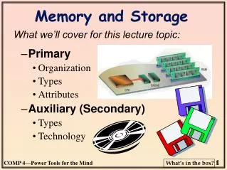
Memory versus Storage • “Memory” refers to semiconductor devices of the kinds we’ve been discussing (RAM, ROM, Flash). • “Storage” refers to non-semiconductor non-volatile devices used to store huge quantities of data. Major categories include: • Magnetic disk (such as computer hard drives) • Magnetic tape • Optical disk (CDs and DVDs)
Magnetic Hard Drive The magnetic hard drive is the backbone of computer mass storage and is applied to other devices such as digital video recorders. Capacities of hard drives have increased exponentially, with 1 TB (1 trillion bytes!) drives available today. Hard drive with cover removed
Optical Storage The compact disk (CD) uses a laser to burn tiny pits into the media. Surrounding the pits are flat areas called lands. The CD can be read using a low-power IR laser that detects the difference between pits and lands. Binary data is encoded with a special method called negative non-return to zero encoding. A change from a pit to a land or a land to a pit represents a binary one, whereas no change represents a zero. A standard 120 mm CD can hold approximately 700 MB of data.