Download
1 / 22
220 likes | 238 Views
Collaborative efforts on new generation Silicon trackers for research in Super B factory, LHC, and future Linear Collider, optimizing materials and resolution. KEK & LPNHE teams aim to improve sensors, FE/DAQ, mechanics, and industry ties.

E N D
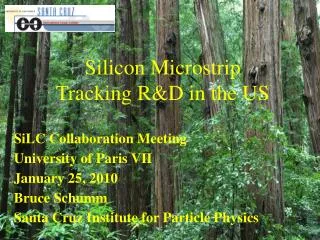
D_RD_4: R&D on the new generation of Large area Silicon tracking systems Toru Tsuboyama & Aurore Savoy-Navarro KEK –LPNHE/IN2P3-CNRS FJPPL Meeting in Paris, May 15-16 2008 R&D4, T. Tsuboyama - A. Savoy Navarro, FJPPL ‘08
The teams • KEK Toru Tsuboyama (KEK) Yasuo Arai (KEK) Yoichi Ikegami (KEK) Takeo Kawasaki (Niigata Uni.) Osamu Tajima (KEK) • LPNHE –IN2P3/CNRS Aurore Savoy-Navarro (LPNHE) CatalinCiobanu (LPNHE) Jacques David (LPNHE) Didier Imbault (LPNHE) Frederic Kapusta (LPNHE) Thanh Hung Pham (LPNHE) Mediatheque in Sendai Bibliotheque Mitterand R&D4, T. Tsuboyama - A. Savoy Navarro, FJPPL ‘08
The goals of our collaboration To develop the next generation of the large area Silicon trackers for applications to: Super B factory, LHC upgrades and future Linear Collider with synergy between them all. Main aims: to reduce material budget and improve performances in spatial and momentum resolutions • The main common topics of interest are thus: • New sensors • New FE and DAQ • Improving Mechanics and related issues • Developing collaborations with Industry Presently KEK is concentrating on the SuperKEKBproject and LPNHE on the ILC project but exploiting the synergy between them both and with the LHC construction and forthcoming upgrades. R&D4, T. Tsuboyama - A. Savoy Navarro, FJPPL ‘08
LARGE AREA TRACKING SYSTEMS: examples & synergy SiD ILD now R&D4, T. Tsuboyama - A. Savoy Navarro, FJPPL ‘08
KEK side Preparation of upgrade of the Belle Si vertex detector (SVD). The motivations of the SVD upgrade for the Super B factory are : • To measure the precise CP violation parameters. • To give strict constraints to the unitarity triangle measurement. • Any deviation from the S.M. prediction suggests a contribution from new physics. • A simulation study tells that the ambiguity of DSSD sensor position and direction (alignment) would limit the precision of CP violation measurement. Stable SVD structure and reliable alignment methods. • Improve the acceptance for Ks • The decay mode B K(*) g is sensitive to contribution from new interaction for example SUSY. Only Ks can be used to reconstruct the B decay vertex. Large area DSSD with thickness < 300 mm. • Improve the tolerance to 20 times background hits from beam. • Beam current would amount to ~10 A (Now KEKB is operated at ~3A ). Performance of ASICS developed for LHC Si strip detectors are appropriate. • The upgrade would start in 2009 and Super KEKB commissioning will be done in 2012 in the earliest case. R&D4, T. Tsuboyama - A. Savoy Navarro, FJPPL ‘08
KEK Activities in 2007 • The Japan side was not funded by FJPPL 2007 and thus FJPPL activities are rather limited.γγ • Participated in SiLC meeting in Torino (Dec 2007) • Fruitful to understand the activity of ILC silicon tracker and synergy between projects • Activities by Belle Silicon Vertex Detector (SVD) group. • Very practical studies as the construction will start in 2009. • Evaluation of large area DSSD • Samples from MICRON semiconductor (UK) were obtained • 300 μm thick, double sided, from 6” wafers. • IV measurement and inter-strip capacitance measurement in progress. • Will be assembled with APV 25 ASIC (CMS FE chip). • Intense simulation study for designing SVD for Super KEKB. • Important physics channels are selected and optimization was done in each cases. • B π+ π-(high momentum tracks), B D D (High multiplicity event) B D* D* (Slow pions) and B Ks π0γ(vertexing with Ks only) • Optimization of SVD structure, DSSD position, material budget, DSSD readout pitch is performed. R&D4, T. Tsuboyama - A. Savoy Navarro, FJPPL ‘08
Advertisement: SOI pixel sensor R&D • Leader: Y. Arai (KEK) • Activity started as one of KEK detector R&D projects in 2005. • Three multi-project wafers have been submitted (2005, 2006 and 2007) to OKI 0.15/0.20 mm SOI CMOS. • Multiple-Project Wafer: KEK, Jaxa, Hawaii, FNAL and LBL have joined. • Arai will welcome new participations from France. • This project is also of interest for Super KEKB: • SVD in Super KEKB requires a monolithic pixel sensor in order to reduce occupancy caused by beam-induced background hits. R&D4, T. Tsuboyama - A. Savoy Navarro, FJPPL ‘08
Development of a pixel sensor Cluster energy distributions With 90Sr b source • Prototype pixel based on SOI tech. • Periodical readout and reset is necessary • Evaluation of the pixel structure. • 128x128 20 mmx20 mm pixels. • Response to pulsed laser and MIP particles was confirmed. • A prototype pixel sensor for the Belle SVD upgrade was submitted in Dec 2007. • Continuous sampling + comparator + digital pipeline. • The evaluation will start soon. Trigger Latency Response to Laser Light R&D4, T. Tsuboyama - A. Savoy Navarro, FJPPL ‘08
KEK activities in 2008 • Common interests of SiLC R&D and the Belle SVD upgrade. • Alignment: The silicon strip sensors with IR-transparent part, being tested by SiLC, is a solution for the detector alignment of Super KEKB SVD. • The large area sensor: becoming important in the design of the upgrade of Belle SVD. • Mechanical structure: Light weight, stable and precision way of designing and machining should be developed. • Pixel sensor R&D will be continued to aim a pixel sensor that can be installed to Super KEKB. • Development of monolithic sensor is also a common interests between us. Exchange information will be continued. R&D4, T. Tsuboyama - A. Savoy Navarro, FJPPL ‘08
LPNHE side Work performed within the SiLC international R&D Collaboration and EUDET European Funded R&D project. Most of the work presented here is achieved in collaboration with SiLC collaborating Institutes. Not much funding from FJPPL in 2007 (5 K€) spent for FJPPL 2007 (2 people). Visit HPK at Hamamatsu City in May 2007 while also attending FJPPL’07 (ASN) ASN’s visit at KEK in March 2008: meeting with Y. Arai, J. Haba and T. Tsuboyama Organisation of the VIth SiLC collaboration meeting in Torino December 2007; invitation of T. Tsuboyama to present the Silicon developments at KEK . Fruitful exchanges. Exchanges between SuperB factories (SuperKEKB & Frascati, LHC & SLHC and ILC). See http://www.silc.to.infn.it/ Torino Dec’07 R&D4, T. Tsuboyama - A. Savoy Navarro, FJPPL ‘08
LPNHE R&D on sensors • Classical sensors: Strips sensors: thinner, large wafer & small pitch, SSD (possibly DSSD for innermost layers). • Novel technologies: • 3D planar new μstrips (VTT Finland) FOXFET DC biaising, 6’’ wafers (5x5cm2 sensors) Edgeless, low V, thinner, rad hard. Ready by June 08 Bottom of the etched trend • 3D pixels (starting): the extension of pixel tech is considered both for LHC upgrades or ILC designs • Epitaxial SOI sensors (also under consideration: see KEK+OKI) New HPK sensors: 6’’, 320μm, 50μm pitch Test structures for detailed quality check of sensor functioning parameters. R&D4, T. Tsuboyama - A. Savoy Navarro, FJPPL ‘08
LPNHE R&D on Electronics Advancement in a F.E. Readout fully digitized in 130 nm deep sub micron CMOS technology . A new version will be sent for foundry (UMC) May 30th , with 86 channels/chip in 5x10mm2. B.U. and LPNHE A previous version with 4 ch/chip successfully tested In 2007 at Lab test bench (see next slide) and CERN test beam : R&D4, T. Tsuboyama - A. Savoy Navarro, FJPPL ‘08
Another interesting asset: use fast track reconstruction (FTK) to trigger (CDF&ATLAS ) or real time preprocessing at ILC The Pattern Bank • Complete pattern recognition on the fly as the silicon data passes by using pre-stored bank of possible hit patterns. • CDF: 32K patterns/phi sector → 15M in ATLAS • made possible by advances in -electronics in past decade • currently 640K patterns in CDF upgrade as step to ATLAS size • An impressive asset for Physics! Just a sketch; all silicon layers are used. ATLAS CDF By courtesy M. Shochet & al.
INLINE PITCH ADAPTER Goal: developing new routing and inline pitch technology for FE chip onto the strips(NdA + MTA) 1st attempt: SiTR_130-86 chip and new HPK sensors Chip 86 voies COLLABORATION HPK/LPNHE-IN2P3 Decrease %X0: NO hybride & pitch adapter 1st approach (2008-2009): Chip directly routed onto the strips by bump bonding HPK: sensor + bonding of the chip IN2P3: chip 86 channels performance tests comparing new connection wrt hybrid Demonstrator: end 2008, production 2009 Chip bonded sensors at the price of usual sensors Futur: 3D vertical inter connects chip/µstrips (starting jointeffort FNAL-IN2P3) R&D4, T. Tsuboyama - A. Savoy Navarro, FJPPL ‘08
Mechanics related issues • Mechanics play a central role also in lowering the material budget. • Among the main topics of common interest: • New composite materials to build the mechanical structures • Alignment • Cooling R&D4, T. Tsuboyama - A. Savoy Navarro, FJPPL ‘08
AMS-like approach: baseline version: Minimum set of changes for any SiLC sensors. For instance, for the new HPK sensors Implemented: • ~10 mm window where Al back-metalization has been removed Suggested (not cost effective for small batches): • Strip width reduction (in alignment window) • Alternate strip removal (in alignment window) Alignment: 2-fold approach and CNM/CSIC Alignment is crucial for high spatial resolution Asset: fully integrated in Si tracking, no additional material R&D on transparent Silicon μstrip sensors: • Together with IMB-CNM (Barcelona) design, build and test new IR-transparent Silicon microstrip detectors. • Consider option of aluminum electrodes or transparent electrodes. Realistic sensor simulations: very interesting studies/results Test bench in development and alignment prototype for TB2008 R&D4, T. Tsuboyama - A. Savoy Navarro, FJPPL ‘08
COOLING: interesting developments by Bosi et al (Pisa) By courtesy of F. Bosi R&D4, T. Tsuboyama - A. Savoy Navarro, FJPPL ‘08
TEST BEAM ACTIVITIES Test beam at SPS-H6 at CERN, Oct 07 EUDET telescope SiLC beam Test beam schedule from 08-10 test beam@/with KEK? R&D4, T. Tsuboyama - A. Savoy Navarro, FJPPL ‘08
Connections with Industry The Si tracking activity implies developing close collaborative contacts with Industrial firms; the collaboration between our 2 teams includes exchanging expertise and knowledge. • KEK side Micron (DSSD strips) Korean Si sensors OKI (SOI) • LPNHE side HPK (new SSD & inline pitch adapter) Korean Si sensors (new strips) Canbera S.C(DSSD +novel Si tech) Leti (?) (SOI) Firms for new composite materials, cabling are also under investigation on both sides and expertise could be shared R&D4, T. Tsuboyama - A. Savoy Navarro, FJPPL ‘08
Budget request for 2008Main aim: Jointly organized Workshop at KEK on Si tracking French team Japanese team Total of 600K Yens, for: 2 travels Additional funding would be allocated for the organization of the workshop in KEK Total of 15.5 K Euros, for: • covering travel expenses (5 people) • contribution to the workshop • Shipping material The Workshop at KEK will gathered representatives of other SiLC Institutes, from Industries and Applied Laboratories with which we are currently collaborating. Material shipping: for sending material. R&D4, T. Tsuboyama - A. Savoy Navarro, FJPPL ‘08
Concluding remarks • Despite almost no FJPPL funding in 2007, the collaboration between KEK and LPNHE was launched and developed in 2007 through short visits and attendance to the SiLC Collaboration Meeting in Torino. It is essential to have the financing for exchanged visits to further develop our collaboration. • There is a synergy in the development of Si tracking systems applied to SuperB factories, LHC upgrades and SLHC, the future LCs: ILC and CLIC, on the main issues: => sensors: based on ‘’traditional’’ strips or on novel technologies (3D-based) => FE electronics: based on VDSM and fully processed signal at the FE => Mechanics: new materials, novel support architectures, alignment, cooling, cabling Differences between machines & environmental conditions are indeed a stimuli to work out and understand in depth the solutions in every R&D aspect> Our collaboration fully subscribe to this framework • The collaboration with industrial firms is another important aspect of this R&D : our collaboration intends to push further joint efforts with both Asian and E.U.firms • The programme of the proposed Workshop at KEK will follow these lines. R&D4, T. Tsuboyama - A. Savoy Navarro, FJPPL ‘08