
Understanding MOSFET Technology in Microelectronics
Explore the operation, structure, and applications of MOSFET technology in modern electronic devices. Learn about thresholds, operation modes, and characteristics of three-terminal semiconductor devices.

Understanding MOSFET Technology in Microelectronics
E N D
Presentation Transcript
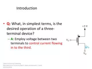
Introduction • Q:What, in simplest terms, is the desired operation of a three-terminal device? • A:Employ voltage between two terminals to control current flowing in to the third. Oxford University Publishing Microelectronic Circuits by Adel S. Sedra and Kenneth C. Smith (0195323033)
Introduction note: MOSFET is more widely used in implementation of modern electronic devices • Q:What are two major types of three-terminal semiconductor devices? • metal-oxide-semiconductor field-effect transistor(MOSFET) • bipolar junction transistor(BJT) • Q:Why are MOSFET’s more widely used? • size (smaller) • ease of manufacture • lesser power utilization • MOSFET technology • It allows placement of approximately 2 billion transistors on a single IC • backbone of very large scale integration (VLSI) • It is considered preferable to BJT technology for many applications. Oxford University Publishing Microelectronic Circuits by Adel S. Sedra and Kenneth C. Smith (0195323033)
5.1. Device Structure and Operation • Figure 5.1. shows general structure of the n-channel enhancement-type MOSFET Figure 5.1: Physical structure of the enhancement-type NMOS transistor: (a) perspective view, (b) cross-section. Note that typically L = 0.03um to 1um, W = 0.1um to 100um, and the thickness of the oxide layer (tox) is in the range of 1 to 10nm. Oxford University Publishing Microelectronic Circuits by Adel S. Sedra and Kenneth C. Smith (0195323033)
5.1.3. Creating a Channel forCurrent Flow • Q: What happens if (1) source and drain are grounded and (2) positive voltage is applied to gate? Refer to figure to right. • step #1:vGS is applied to the gate terminal, causing a positive build up of positive charge along metal electrode. • step #2:This “build up” causes free holes to be repelled from region of p-type substrate under gate. Figure 5.2: The enhancement-type NMOS transistor with a positive voltage applied to the gate. An n channel is induced at the top of the substrate beneath the gate Oxford University Publishing Microelectronic Circuits by Adel S. Sedra and Kenneth C. Smith (0195323033)
Q: What happens if (1) source and drain are grounded and (2) positive voltage is applied to gate? Refer to figure to right. • step #3:This “migration” results in the uncovering of negative bound charges, originally neutralized by the free holes • step #4:The positive gate voltage also attracts electrons from the n+ source and drain regions into the channel. Figure 5.2: The enhancement-type NMOS transistor with a positive voltage applied to the gate. An n channel is induced at the top of the substrate beneath the gate Oxford University Publishing Microelectronic Circuits by Adel S. Sedra and Kenneth C. Smith (0195323033)
5.1.3. Creating a Channel forCurrent Flow Vtn is used for n-type MOSFET, Vtp is used for p-channel • threshold voltage (Vt) – is the minimum value of vGS required to form a conducting channel between drain and source • typically between 0.3 and 0.6Vdc • field-effect – when positive vGS is applied, an electric field develops between the gate electrode and induced n-channel – the conductivity of this channel is affected by the strength of field • SiO2 layer acts as dielectric • effective / overdrive voltage – is the difference between vGS applied and Vt. • oxide capacitance (Cox) – is the capacitance of the parallel plate capacitor per unit gate area (F/m2) Oxford University Publishing Microelectronic Circuits by Adel S. Sedra and Kenneth C. Smith (0195323033)
avOV avDS The voltage differential between both sides of n-channel increases with vDS. Oxford University Publishing Microelectronic Circuits by Adel S. Sedra and Kenneth C. Smith (0195323033) Figure 5.5: Operation of the e-NMOS transistor as vDS is increased.
note that we can define total charge stored in channel |Q| as area of this trapezoid note the average value Figure 5.6(a): For a MOSFET with vGS = Vt + vOVapplication of vDS causes the voltage drop along the channel to vary linearly, with an average value of vDS at the midpoint. Since vGD > Vt, the channel still exists at the drain end. (b) The channel shape corresponding to the situation in (a). While the depth of the channel at the source is still proportional to vOV, the drain end is not. Oxford University Publishing Microelectronic Circuits by Adel S. Sedra and Kenneth C. Smith (0195323033)
5.1.6. Operation for vDS >> vOV pinch-off does not mean blockage of current • In section 5.1.5, we assume that n-channel is tapered but channel pinch-off does not occur. • Trapezoid doesn’t become triangle for vGD > Vt • Q:What happens if vDS > vOV? • A: MOSFET enters saturation region. Any further increase in vDS has no effect on iD. Figure 5.8: Operation of MOSFET with vGS = Vt + vOV as vDS is increased to vOV. At the drain end, vGD decreases to Vt and the channel depth at the drain-end reduces to zero (pinch-off). At this point, the MOSFET enters saturation more of operation. Further increasing vDS (beyond vOV) has no effect on the channel shape and iD remains constant. Oxford University Publishing Microelectronic Circuits by Adel S. Sedra and Kenneth C. Smith (0195323033)
saturation occurs once vDS > vOV Oxford University Publishing Microelectronic Circuits by Adel S. Sedra and Kenneth C. Smith (0195323033)
5.1.7. The p-Channel MOSFET • Figure 5.9(a) shows cross-sectional view of a p-channel enhancement-type MOSFET. • structure is similar but “opposite” to n-channel • complementary devices – two devices such as the p-channel and n-channel MOSFET’s. Figure 5.9(a): Physical structure of the PMOS transistor. Note that it is similar to the NMOS transistor shown in Figure 5.1(b), except that all semiconductor regions are reversed in polarity. (b) A negative voltage vGS of magnitude greater than |Vtp| induces a p-channel, and a negative vDS causes a current iD to flow from source to drain. Oxford University Publishing Microelectronic Circuits by Adel S. Sedra and Kenneth C. Smith (0195323033)
5.1.8. Complementary MOS or CMOS • CMOS employs MOS transistors of both polarities. • more difficult to fabricate • more powerful and flexible • now more prevalent than NMOS or PMOS Oxford University Publishing Microelectronic Circuits by Adel S. Sedra and Kenneth C. Smith (0195323033)
Figure 5.10: Cross-section of a CMOS integrated circuit. Note that the PMOS transistor is formed in a separate n-type region, known as an n well. Another arrangement is also possible in which an n-type body is used and the n device is formed in a p well. Not shown are the connections made to the p-type body and to the n well; the latter functions as the body terminal for the p-channel device. n-well is added to allow generation of p-channel p-type semiconductor provides the MOS body (and allows generation of n-channel) SiO2 is used to isolate NMOS from PMOS Oxford University Publishing Microelectronic Circuits by Adel S. Sedra and Kenneth C. Smith (0195323033)
Oxford University Publishing Microelectronic Circuits by Adel S. Sedra and Kenneth C. Smith (0195323033)
5.2.2. The iD-vGS Characteristic • Q:What is one problem with (5.21)? • A:It is nonlinear w/ respect to vOV … however, this is not of concern now. • In effect, it becomes a voltage-controlled current source. • This is key for amplification. • Refer to (5.21). Figure 5.14: The iD-vGS characteristic of an NMOS transistor operating in the saturation region. The iD-vOV characteristic can be obtained by simply re-labeling the horizontal axis, that is, shifting the origin to the point vGS = Vtn. Oxford University Publishing Microelectronic Circuits by Adel S. Sedra and Kenneth C. Smith (0195323033)
5.2.2. The iD-vGS Characteristic • The view of transistor as CVCS is exemplified in figure 5.15. • This circuit is known as the large-signal equivalent circuit. • Current source is ideal. • Infinite output resistance represents independent, in saturation, of iD from vDS.. note that, in this circuit, iD is completely independent of vDS (because no shunt resistor exists) Figure 5.15: Large-signal equivalent-circuit model of an n-channel MOSFET operating in the saturation Oxford University Publishing Microelectronic Circuits by Adel S. Sedra and Kenneth C. Smith (0195323033)
5.2.4. Finite Output Resistance in Saturation • Q:How do we account for “this effect” in iD? • A:Refer to (5.23). • A:Addition of finite output resistance (ro). Figure 5.16: Increasing vDS beyond vDSsat causes the channel pinch-off point to move slightly away from the drain, thus reducing the effective channel length by DL Figure 5.18: Large-Signal Equivalent Model of the n-channel MOSFET in saturation, incorporating the output resistance ro. The output resistance models the linear dependence of iD on vDS and is given by (5.23) Oxford University Publishing Microelectronic Circuits by Adel S. Sedra and Kenneth C. Smith (0195323033)
5.2.4. Finite Output Resistance in Saturation • Q:How is ro defined? • step #1:Note that ro is the 1/slope of iD-vDS characteristic. • step #2:Define relationship between iD and vDS using (5.23). • step #3:Take derivative of this function. • step #4:Use above to define ro. • Note that ro may be defined in terms of iD, whereiD does not take in to account channel length modulation… Oxford University Publishing Microelectronic Circuits by Adel S. Sedra and Kenneth C. Smith (0195323033)
5.2.4. Finite Output Resistance in Saturation • Q: What is l? • A:A device parameter with the units of V -1, thevalue of which depends on manufacturer’s design and manufacturing process. • much larger for newer tech’s • Figure 5.17 demonstrates the effect of channel length modulation on vDS-iD curves • In short, we can draw a straight line between VA and saturation. Figure 5.17: Effect of vDS on iD in the saturation region. The MOSFET parameter VA depends on the process technology and, for a given process, is proportional to the channel length L. Oxford University Publishing Microelectronic Circuits by Adel S. Sedra and Kenneth C. Smith (0195323033)
5.4.2. Voltage Transfer Characteristic • voltage transfer characteristics (VTC) –plot of out voltage vs. input • three regions exist in VTC • vGS < Vtcut off FET • vOV = vGS – Vt < 0 • ID = 0 • vDS ??? vOV • vout = vDD • Vt < vGS < vDS + Vt saturation • vOV= vGS – Vt> 0 • ID = ½ kn(vGS – Vt)2 • vDS >> vOV • vout = VDD – IDRD • vDS + Vt < vGS < VDD triode • vOV= vGS – Vt> 0 • ID = kn(vGS – Vt – vDS)vDS • vDS > vOV • vout = VDD – IDRD Figure 5.27: (b) the voltage transfer characteristic (VTC) of the amplifier from previous slide Oxford University Publishing Microelectronic Circuits by Adel S. Sedra and Kenneth C. Smith (0195323033)
5.4.3: Biasing the MOSFET to Obtain Linear Amplification linear amplification around Q in saturation region • bias point / dc operating pt. (Q) = point of linearization for MOSFET • also known as quiescent point • Q: how will Q help us? • because VTC is linear near Q, we may perform linear amplification of signal << Q Figure 5.28: biasing the MOSFET amplifier at point Q located on segment AB of VTC Oxford University Publishing Microelectronic Circuits by Adel S. Sedra and Kenneth C. Smith (0195323033)
Q:How is linear gain achieved? Figure 5.29: The MOSFET amplifier with a small time-varying signal vgs(t) superimposed on the dc bias voltage vGS. The MOSFET operates on a short almost-linear segment of the VTC around the bias point Q and provides an output voltage vds = Avvgs As long as vgs(t) is small, its effect on vDS(t) will be linear – facilitating linear amplification. Oxford University Publishing Microelectronic Circuits by Adel S. Sedra and Kenneth C. Smith (0195323033)
5.4.4. Small-Signal Gain • Equation (5.38) is another version of (5.37) which incorporates (5.17). • It demonstrates that gain is ratio of: • voltage drop across RD • half of over voltage Oxford University Publishing Microelectronic Circuits by Adel S. Sedra and Kenneth C. Smith (0195323033)


