Download
1 / 22
240 likes | 402 Views
Chapter 7 Flip-Flops, Registers, and Counters. Sequential circuits – Logic circuits in which the values of the outputs depend not only on the present values of the inputs but also on the past behavior of the circuit. Flip-flop- A clocked element which can remember and store 1-bit of information.

E N D
Chapter 7Flip-Flops, Registers, and Counters Sequential circuits – Logic circuits in which the values of the outputs depend not only on the present values of the inputs but also on the past behavior of the circuit. Flip-flop- A clocked element which can remember and store 1-bit of information.
Motivation: Set Sensor ¤ On Off Memory Alarm element Reset Figure 7.1. Control of an alarm system. Alarm turned on when On/Off =1, and is off when On/Off =0. Once triggered, alarm stays on till manually reset. The circuit requires memory element.
A B Figure 7.2. A simple memory element. A feedback loop with even number of inverters. If A = 0, B =1 or when A = 1, B =0, circuit is not useful due to the lack of a mechanism for changing its state.
Reset Set Q Figure 7.4. A memory element with NOR gates.
t su t h Clk D Q Figure 7.9. Setup and hold times. Setup time tsu: The minimum time that the input signal must be stable prior to the edge of the clk signal. Hold time th: The minimum time that the input signal must be stable prior to the edge of the clk signal.
Master Slave Q Q m s Q Q D D Q D Clk Clk Clock Q Q Q (a) Circuit Clock D Q m Q = Q s (b) Timing diagram Q D Q (c) Graphical symbol Figure 7.10. Master-slave D flip-flop.
Q D Clock Q (b) Graphical symbol Figure 7.11. A positive-edge-triggered D flip-flop.
Q D D Q a Clock Q Q Clk a Q D Q b Q Q b Q D Q c Q Q c (a) Circuit Clock D Q a Q b Q c (b) Timing diagram Figure 7.12. Comparison of level-sensitive and edge-triggered D storage elements.
Preset Q D Q Clear (b) Graphical symbol Figure 7.13. Master-slave D flip-flop with Clear and Preset.
Q D Q T Q Q Clock (a) Circuit ( ) Q t + 1 T Q T ( ) 0 Q t ( ) 1 Q t Q (b) Characteristic table (c) Graphical symbol Clock T Q (d) Timing diagram Figure 7.16. T flip-flop.
J Q D Q K Q Q Clock (a) Circuit Q ( t + 1 ) J K 0 0 Q ( t ) J Q 0 1 0 1 0 1 K Q 1 1 Q ( t ) (b) Characteristic table (c) Graphical symbol Figure 7.17. JK flip-flop.
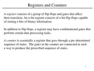
Registers and Counters An n-bit register is a cascade of n flip-flops and can store an n-bit binary data. A counter can count occurrences of events and can generate timing intervals for control purposes.
Q Q Q Q 1 2 3 4 In Out Q Q Q Q D D D D Clock Q Q Q Q (a) Circuit Q Q Q Q = Out In 1 2 3 4 t 1 0 0 0 0 0 t 0 1 0 0 0 1 t 1 0 1 0 0 2 t 1 1 0 1 0 3 t 1 1 1 0 1 4 t 0 1 1 1 0 5 t 0 0 1 1 1 6 t 0 0 0 1 1 7 (b) A sample sequence Figure 7.18. A simple shift register.
Parallel output Q Q Q Q 3 2 1 0 Q Q Q Q D D D D Q Q Q Q Serial Clock Shift/Load input Parallel input Figure 7.19. Parallel-access shift register. Performs both as a series-to-parallel and a parallel-to-series converter
0 0 0 0 0 1 0 1 0 1 1 0 1 Q Q Q T T T Clock Q Q Q Q Q Q 0 (a) Circuit 1 2 Q1 is connected to clk, Q2 and Q3 are clocked by Q’ of the preceding stage (hence called asynchronous or ripple counter). Clock Q 0 Q 1 Q 2 Count 0 1 2 3 4 5 6 7 0 (b) Timing diagram Figure 7.20. A three-bit up-counter.
1 Q Q Q T T T Clock Q Q Q Q Q Q 0 1 2 (a) Circuit Clock Q 0 Q 1 Q 2 Count 0 7 6 5 4 3 2 1 0 (b) Timing diagram Q1 is connected to clk, Q2 and Q3 are clocked by Q of the preceding stage. (asynchronous or ripple counter). Figure 7.21. A three-bit down-counter.
Clock cycle Q Q Q 2 1 0 Q changes 1 0 0 0 0 Q changes 2 1 0 0 1 2 0 1 0 3 0 1 1 4 0 0 1 5 1 0 1 6 1 0 1 7 1 1 1 8 0 0 0 Q0 changes with clk, Q2 changes when previous state of Q0 was 1, and Q3 changes when pervious state of Q1 and Q0 were 1. Table 7.1. Derivation of the synchronous up-counter.
1 Q Q Q Q T T T T Q Q Q Q 0 1 2 3 Clock Q Q Q Q (a) Circuit Clock Q 0 Q 1 Q 2 Q 3 Count 0 1 2 3 4 5 6 7 8 9 10 11 12 13 14 15 0 1 (b) Timing diagram Figure 7.22. A four-bit synchronous up-counter.
Enable Q Q Q Q T T T T Clock Q Q Q Q Clear Figure 7.23. Inclusion of Enable and Clear capability.