Download
1 / 31
320 likes | 479 Views
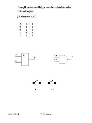
JA element AND. Loogikaelemendid ja nende valmistamise tehnoloogiad. X 1 X 2 Y 0 0 0 0 1 0 0 0 1 1 1. x 1. &. x 1. y. y. x 2. x 2. x 1. x 2. VÕI element OR. X 1 X 2 Y 0 0 0 0 1 1 0 1 1 1 1. x 1. 1. x 1. y. y. x 2. x 2. x 1. x 2. EI element NOT. X Y

E N D
JA elementAND Loogikaelemendid ja nende valmistamise tehnoloogiad • X1 X2 Y • 0 0 0 • 0 1 0 • 0 0 • 1 1 1 x 1 & x 1 y y x 2 x 2 x 1 x 2 T. Evartson
VÕI elementOR • X1 X2 Y • 0 0 0 • 0 1 1 • 0 1 • 1 1 1 x 1 1 x 1 y y x 2 x 2 x 1 x 2 T. Evartson
EI elementNOT X Y 0 1 1 0 1 y x y x T. Evartson
MOSFET trasistorid (nMOS, pMOS ja CMOS tehnoloogiad) n MOS transistor Pais Gate - G Läte Source - S Neel Drain - D Silicon select gate n p p +VDD +VDD D D G=L G=H S S GND GND p-MOS transistor +VDD +VDD S S G=L G=H D D GND GND T. Evartson
EI elemendi realiseerimine CMOS tehnoloogias X Y 0 1 1 0 1 x y y x +VDD +VDD +VDD y y y x UX=H UX=L GND GND GND n-MOS transistor p-MOS transistor = = T. Evartson
Lülitumine CMOS tehnoloogias T. Evartson
Dünaamilised karakteristikud T. Evartson
JA-EI element NAND • X1 X2 Y • 0 0 1 • 0 1 1 • 0 1 • 1 1 0 x 1 y x 2 x 1 & x 1 & 1 y y x 2 x 2 +VDD y x 1 x 2 GND T. Evartson
VÕI-EI element NOR • X1 X2 Y • 0 0 1 • 0 1 0 • 0 0 • 1 1 0 x1 y x2 x 1 1 x 1 1 1 y y x 2 x 2 +VDD x 1 x 2 y GND T. Evartson
CMOS tehnoloogia JA ja VÕI elemendid +VDD y x 1 x 2 GND +VDD x 1 x 2 y GND T. Evartson
Bipolaarsed tehnoloogiad (DL-tehnoloogia Diode Logic) n p 0 +VDD 0 +VDD +VD x 1 Y & X1 y x 2 X2 GND +VD +VD Y=L Y=H X1=H X1=H X2=H X2=L GND GND T. Evartson
DL T. Evartson
Bipolaarne transistor n-p-n transistor Baas Base Emitter Emitter Kollektor Collector n p n +Vc +Vc C C B=L B=H E E GND GND p-n-p transistor Baas Base Emitter Emitter Kollektor Collector p n p +Vc +Vc E E B B C C GND GND T. Evartson
DTL , RTL T. Evartson
TTL (Transistor Transistor Logic) T. Evartson
ECL T. Evartson
STTL T. Evartson
IIL T. Evartson
Korpus T. Evartson
Kolme olekuga väljund (Three State Output) • E X Y • 0 - Z • 0 0 • 1 1 1 E X Y +Vdd E & b Y X 1 c a 1 GND T. Evartson
Montaazi loogika Wired Logic +Vc x1 Y1 +Vdd GND AND Y Y2 x2 +Vdd GND Y3 x3 GND T. Evartson
Montaazi loogika probleemid +Vc R x1 Y1 +Vdd GND R AND Y Y2 x2 +Vdd GND R Y3 x3 GND T. Evartson
Montaazi loogika ja avatud suudme/kollektoriga elementidel +Vc x1 Y1 GND AND Y Y2 x2 GND x3 Y3 GND T. Evartson
Avatud kollektoriga element T. Evartson
Kokku ühendatud CMOS väljundid +VDD NAND y1 x 1=H x 2=L y +VDD GND NAND x 3=H y2 x 4=H GND T. Evartson
Avatud neeluga väljund ja montaazi loogikaOpen Drainan Output and Wired Logic +Vdd Y x 1 y x1 x 2 +VDD x2 GND x1 Y1 x2 AND GND Y Y2 x3 x4 GND Y3 x5 x6 GND T. Evartson
Schmitti triger T. Evartson
Ajadiagramm T. Evartson