DC Power Supplies: Basics & Applications
750 likes | 771 Views
Learn about the basics of DC power supplies, including transformers, rectifiers, and regulators. Understand the operation of half-wave rectifiers and how they convert AC to DC voltage, maintaining a constant output. Explore the components and functions of a DC power supply system, essential for electronic circuits in various applications.

DC Power Supplies: Basics & Applications
E N D
Presentation Transcript
1-1 The Basic DC Power Supply • Power supply is a group of circuits that convert the standard ac voltage (120 V, 60 Hz) provided by the wall outlet to constant dc voltage. • The voltage produced is used to power all types of electronic circuits including: • Consumer electronics (ex: radio, television, DVD, etc.) • Computers • Industrial controllers • Most laboratory instrumentation systems and equipment • The dc voltage level required depends on the application, but most applications require relatively low voltage. • There are two basic types of power supplies: a linear power supplyanda switching power supply. Thesecomponents are described as follows: • A linear power supply is one that provides a constant current path between its input and its load. • A switching power supply provides an intermittent current path between its input and its output.
1-1 The Basic DC Power Supply(cont.) The basic function of a DC power supply is to convert an AC voltage to a constant DC voltage (AC DC) Maintains a constant dc voltage Eliminates the fluctuations - produce smooth dc voltage Either half or full-wave rectifier convert ac input voltage to a pulsating dc voltage. (a) Complete power supply with transformer, rectifier, filter, and regulator (b) Half-wave rectifier Fig. 2-1: Block diagram of a dc power supply with a load and rectifier.
1-1 The Basic DC Power Supply(cont.) Transformer • A transformer is a device that changes ac electric power at one voltage level to ac electric power at another voltage level through the action of a magnetic field. • Simple transformer consist of: 1. Primary winding (input winding) 2. Secondary winding (output winding) 3. Magnetic core • If the secondary has more turns than the primary, the output voltage across the secondary will be higher and the current will be smaller. If the secondary has fewer turns than the primary, the output voltage across the secondary will be lower and the current will be higher. • The core has a function to concentrate the magnetic flux. Fig.2-2: The general arrangement of a transformer
2-1 The Basic DC Power Supply(cont.) NS NS NS NP NP NP + + + + + + 120 Vac 240 Vac 120 Vac 30 Vac 120 Vac 120 Vac - - - - - - There are three types of transformers: step-up, step-down,andisolation. These components are described as follows: • The step-up transformer provides a secondary voltage that is greater than the primary voltage. Ex: a step-up transformer may provides a 240 Vac output with a 120 Vac input. • The step-down transformer provides a secondary voltage that is less than the primary voltage. Ex: a step-down transformer may provides a 30 Vac output with a 120 Vac input. • An isolation transformer provides an output voltage that is equal to the input voltage. This type of transformer is used to isolate the power supply electrically from the ac power line. Step-up Step-down Isolation (a) (c) (b) Fig.2-3
2-1 The Basic DC Power Supply(cont.) The turns ratio of a transformer is equal to the voltage ratio of the component and since, the voltage ratio is the inverse of the current ratio. By formula: (2-1) where NSec = the number of turns in the secondary NPri = the number of turns in the primary VSec = the secondary voltage VPri = the primary voltage ISec = the secondary current IPri = the primary current By the equation (2-1) can be stated that: • Step-down transformer secondary current is greater than its primary current (ISec > IPri). • Step-up transformer secondary current is less than its primary current (IPri > ISec).
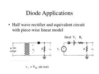
2-2 Half-Wave Rectifiers Diode – ability to conduct current in one direction and block current in other direction used in circuit called RECTIFIER (ac dc) Objective: • Discuss the operation of half-wave rectifiers • Describe a basic dc power supply & half-wave rectifications • Determine the average value, VAVG of half-waves rectified voltage • Discuss the effect of barrier potential, VP on a half-wave rectifier output • Define Peak Inverse Voltage (PIV) • Describe Transformer-couple half-wave rectifier
2-2 Half-Wave Rectifiers (cont.)(The Half-Wave Rectifier) load resistor ac source • A half wave rectifier(ideal) allows conduction for only 180° or half of a complete cycle. • During first one cycle: • -Vin goes positive – diode FB – conduct current • -Vin goes negative – diode RB – no current- 0V • The output frequency is the same as the input (same shape). The average value VDC or VAVG : Ideal diode model -Measure on dc voltmeter
2-2 Half-Wave Rectifiers (cont.)(Effect of the Barrier Potential on the Half-Wave Rectifier Output) • Practical Diode – barrier potential of 0.7V (Si) taken into account. • During +ve half-cycle – Vin must overcome Vpotential for forward bias. • Example 1: Calculate the peak o/p voltage, Vp(out)? The peak o/p voltage:
2-2 Half-Wave Rectifiers (cont.)(Effect of the Barrier Potential on the Half-Wave Rectifier Output) Example 2: Sketch the output V0and determine the output level voltage for the network in above figure.
2-2Half-Wave Rectifiers (cont.)[Peak Inverse Voltage (PIV)] - Peak inverse voltage (PIV) is the maximum voltage across the diode when it is in reverse bias. The diode must be capable of withstanding this amount of voltage.
2-2 Half-Wave Rectifiers (cont.)(Half-Wave Rectifier with Transformer-Coupled Input Voltage) • Transformers are often used for voltage change and isolation. • The turns ratio, n of the primary to secondary determines the output versus the input. • The advantages of transformer coupling: 1) allows the source voltage to be stepped up or down 2) the ac source is electrically isolated from the rectifier, thus prevents shock hazards in the secondary circuit. to couple ac input to the rectifier If n>1, Vsec is greater than Vpri. If n<1, Vsec is less than Vpri. If n=1, Vsec= Vpri.
Example 3: Determine the peak value of output voltage as shown in below Figure.
2-3 Full-Wave Rectifiers(Introduction) Objective: • Explain & Analyze the operation of Full-Wave Rectifier. • Discuss how full wave rectifier differs from half-wave rectifier • Determine the average value • Describe the operation of center-tapped & bridge. • Explain effects of the transformers turns ratio • PIV • Comparison between center-tapped & bridge.
2-3 Full-Wave Rectifiers (cont.)(Introduction) • A full-wave rectifier allows current to flow during both the positive and negative half cycles or the full 360º whereas half-wave rectifier allows only during one-half of the cycle. • The no. of +ve alternations is twice the half wave for the same time interval • The output frequency is twice the input frequency. • The average value – the value measured on a dc voltmeter Twice output 63.7% of Vp
2-3 Full-Wave Rectifiers(i - The Center-Tapped Full-Wave Rectifier) • This method of rectification employs two diodes connected to a secondary center-tapped transformer. • The i/p voltage is coupled through the transformer to the center-tapped secondary. Coupled input voltage
2-3 Full-Wave Rectifiers (cont.)(i - The Center-Tapped Full-Wave Rectifier) • +ve half-cycle input voltage (forward-bias D1 & reverse-bias D2)-the current pass through the D1 and RL • -ve half-cycle input voltage (reverse-bias D1 & forward-bias D2)-the current pass through D2 and RL • The output current on both portions of the input cycle – same direction through the load. • The o/p voltage across the load resistors – full-wave rectifiers
2-3 Full-Wave Rectifiers (cont.)(i - The Center-Tapped Full-Wave Rectifier) -Effect of the Turns Ratio on the Output Voltage- If n=1, Vp(out)=Vp(pri) - 0.7V 2 • Vp(sec)=Vp(pri) If n=2, • In any case, the o/p voltage is always one-half of the total secondary voltage minus the diode drop (barrier potential), no matter what the turns ratio.
2-3 Full-Wave Rectifiers (cont.)(i - The Center-Tapped Full-Wave Rectifier) -Peak Inverse Voltage (PIV)- • Maximum anode voltage: • D1: forward-bias – its cathode is at the same voltage of its anode minus diode drop; This is also the voltage on the cathode of D2. • PIV across D2 : • We know that • Thus;
2-2 Full-Wave Rectifiers (cont.)(ii - The Bridge Full-Wave Rectifier) • It employs four diodes arranged such that current flows in the direction through the load during each half of the cycle. • When Vin +ve, D1 and D2 FB and conduct current. A voltage across RL looks like +ve half of the input cycle. During this time, D3 and D4 are RB. • When Vin –ve, D3 and D4 are FB and conduct current. D1 and D2 are RB. Used 4 diode: 2 diode in forward 2 diode in reverse Without diode drop (ideal diode): 2 diode always in series with load resistor during +ve and –ve half cycle . With diode drop (practical diode):
2-2 Full-Wave Rectifiers (cont.)(ii - The Bridge Full-Wave Rectifier) For ideal diode, PIV = Vp(out) For each diode, 0V (ideal diode) Note that in most cases we take the diode drop into account.
2-3 Power Supply Filters And Regulators(introduction) Objective: • Explain & Analyze the operation & characteristic of power supply filters & Regulators • Explain the purpose of a filter • Describe the capacitor-input filter • Define ripple voltage & calculate the ripple voltage • Discuss surge current in capacitor-input filter • Discuss voltage regulation & integrated circuit regulator
2-4 Power Supply Filters And Regulators (cont.) (introduction) Power Supply Filters • To reduce the fluctuations in the output voltage of half / full-wave rectifier – produces constant-level dc voltage. • It is necessary – electronic circuits require a constant source to provide power & biasing for proper operation. • Filters are implemented with capacitors. Regulators • Voltage regulation in power supply done using integrated circuit voltage regulators. • To prevent changes in the filtered dc voltage/ to fix output dc voltagedue to variations in input voltage or load.
2-4 Power Supply Filters And Regulators (cont.) (introduction) • In most power supply – 60 Hz ac power line voltage is converted to constant dc voltage. • 60Hz pulsating dc output must be filtered to reduce the large voltage variation. • Small amount of fluctuation in the filter o/p voltage - ripple ripple
2-4 Power Supply Filters And Regulators (cont.) (Capacitor-Input Filter) Capacitive Filter • Capacitive filter is simply a capacitor connected in parallel with the load resistance or connected from the rectifier output to ground, as shown in Fig.2-39. • During the positive first quarter-cycle of the input, the diode is forward-biased, allowing the capacitor charges rapidly, as illustrated in Fig.2-39(a). • When the input begins to go negative, the diode is reverse-biased, and the capacitor slowly discharges through the load resistance (Fig.2-39(b)). As the output from the rectifier drops below the charged voltage of the capacitor, the capacitor acts as the voltage source for the load. • During first quarter of the next cycle, as illustrated in part (c), the diode will again become forward-biased when the input voltage exceeds the capacitor voltage. load capacitor
Ripple Voltage Ripple voltage is the fluctuation in the capacitor voltage due to the difference between the charge and discharge times. The difference between the charge and discharge times is caused by two distinct RC time constantin the circuit. One time constant is found as: where R and C are the total circuit resistance and capacitance, respectively. Since it takes five time constants for a capacitor to charge or discharge fully, this time period (T) can be found as:
For example, refer to Fig. 2-40(a), the capacitor charges through the diode. Assuming that diode has a forward resistance of 5 Ω, so the time constant for the circuit is found as: and the total capacitor charge time is found as: The discharge path for the capacitor is through the resistor as shown in Fig. 2-40(b). For this circuit, the time constant is found as: and the total capacitor discharge time is found as:
(a) Charge circuit (b) Discharge circuit Fig.2-40: The basic capacitive filter.
2-4Power Supply Filters And Regulators (cont.) (Capacitor-Input Filter) Ripple Voltage: the variation in capacitor voltage due to the charging and discharging times. The advantage of a full-wave rectifier over a half-wave is quite clear. The capacitor can more effectively reduce the ripple when the time between peaks is shorter. Easier to filter -shorted time between peaks. -smaller ripple.
2-4 Power Supply Filters And Regulators (cont.) (Capacitor-Input Filter) Ripple factor: indication of the effectiveness of the filter [half-wave rectifier] Vr(pp) = peak to peak ripple voltage; VDC = VAVG = average value of filter’s output voltage. • Lower ripple factor better filter [can be lowered by increasing the value of filter capacitor or increasing the load resistance] • For the full-wave rectifier: Vp(rect) = unfiltered peak.
2-4 Power Supply Filters And Regulators (cont.) (Capacitor-Input Filter) Surge Current in the Capacitor-Input Filter: When you first turn on power supply, the filter capacitor has no accumulated charge to oppose Vp(sec). For first instant, the capacitor appears as a short circuit, thus the current through the diodes can momentarily be quite high. To reduce risk of damaging the diodes, a surge current limiting resistor is placed in series with the filter and load. The min. surge Resistor values: IFSM = forward surge current rating specified on diode data sheet.
2-4 Power Supply Filters And Regulators (cont.) (IC Regulators) • Connected to the output of a filtered & maintains a constant output voltage (or current) despite changes in the input, load current or temperature. • Combination of a large capacitor & an IC regulator – inexpensive & produce excellent small power supply • Popular IC regulators have 3 terminals: • input terminal (ii) output terminal (iii) reference (or adjust) terminal • Type number: 78xx (xx –refer to output voltage) i.e 7805 (output voltage +5.0V); 7824 (output voltage +24V)
2-4 Power Supply Filters And Regulators (cont.) (IC Regulators) Regulation is the last step in eliminating the remaining ripple and maintaining the output voltage to a specific value. Typically this regulation is performed by an integrated circuit regulator. There are many different types used based on the voltage and current requirements. Connected to the output of filtered rectifier output Bridge-full wave rectifier Gnd filter regulators Fig. 2-23 : A basic +5.0V regulated power supply
2-4 Power Supply Filters And Regulators (cont.) (Percent Regulations) Percent Regulation The regulation can be stated in a percentage in terms of input (line) regulation or load regulation. • Line regulation specifies how much change occurs in the output voltage for a given change in the input voltage. It is mathematically defined as a ratio of a change in output voltage for a corresponding change in the input voltage expressed as a percentage. • Load regulation specifies how much change occurs in the output voltage over a certain range of load current values, usually from minimum current (no load, NL) to maximum current (full load, FL). It can be mathematically determined with the following formula: (2-31)
2-5 Diode Limiting & Clamping Circuits (Introduction) Objectives: • Analyze the operation of diode limiting, clamping circuit, voltage multipliers and interpret and use diode data sheet. • Determine V of biased limiter & used voltage-divider bias to set limiting level. • Discuss voltage doublers, triplers & quadruples. • Identify V & current ratings. • Determine the electrical characteristics of a diode. • Analyze graphical data • Select an appropriate diode for a given set of specifications.
2-5 Diode Limiting & Clamping Circuits (Diode Limiters) • Diode limiters/clippers – that limits/clips the portion of signal voltage above or below certain level. • Limiting circuits limit the positive or negative amount of an input voltage to a specific value. • 4 basic clipper configuration: • Negative series clipper diode is in series with its load • Positive series clipper • Negative shunt clipper diode is in parallel with its load • Positive shunt clipper
2-5 Diode Limiting & Clamping Circuits (Diode Limiters) Clipper configuration
2-5 Diode Limiters(series clipper/limiter) • Negative series clipper • Diode is forward-biased during +ve alternation of i/p signal. • Diode is reverse-biased when i/p signal is –ve. • Eliminates negatives alternation of its i/p. • Positive series clipper • Diode is reverse-biased during +ve alternation of i/p signal. • Diode is forward-biased when i/p signal is –ve. • Eliminates positive alternation of its input.
2-5Diode Limiters(shunt clipper/limiter) Negative shunt clipper • Reverse-biased diode act as open cct during +ve cycle. • Forward-biased diode act as short cct during –ve cycle. • o/p signal is limit/clip to -0.7V during –ve cycle of i/p signal. Positive shunt clipper • Forward-biased diode when i/p is +ve cycle. • Reverse-biased diode when i/p is in –ve cycle. • o/p signal is limit/clip to +0.7V during +ve cycle of i/p signal.
2-5 Diode Limiting & Clamping Circuits (Diode Limiters) Series clipper Shunt clipper For –ve shunt, when i/p signal +ve cycle, diode is RB (open circuit), thus: During –ve cycle, diode is FB, load voltage is equal to diode forward voltage. VL = -VF = -0.7V For +ve shunt, o/p voltage and current direction are reversed. • When diode in –ve series clipper is FB, load voltage is: VL=Vin – 0.7V • When diode is RB, doesn’t conduct, so: • VL = 0V • +ve series clipper operates the same. The only differences are: • O/p voltage polarities are reversed. VL=-Vin + 0.7V • Current direction through cct are reversed.
Question 4: What would you expect to see displayed on an oscilloscope connected across RL in the limiter shown below.
Solution question 4 The diode is forward biased and conducts when input voltage goes below -0.7V. So, for –ve limiter, the peak output voltage across RL is: The waveform is shown below:
2.5 Diode Limiting & Clamping Circuits (cont.) (Diode Limiters) Biased Limiters : • Use dc biasing source, VBIAS to set limit on the circuit output voltage. • This allow the circuit to clip input waveform at values other than diode forward voltage, 0.7V. • In each circuit, bias voltage is in series with shunt diode. As a result, the diode conducts and clips the i/p waveform when signal voltage equals sum of VF and VBIAS. • 2 type of biased limiter: positive-biased limiter negative-biased limiter • Positive limiter • The voltage at point A must equal VBIAS+0.7V before diode become FB and conduct. • Once diode begin to conduct, voltage at point A is limited to VBIAS+0.7V, so all i/p voltage above this level is clipped off. • Negative limiter • Voltage at point A must go below –VBIAS - 0.7V to forward-bias the diode and initiate limiting action. A positive limiter A negative limiter
2-5 Diode Limiting & Clamping Circuits (cont.) (Diode Limiters) Voltage-Divider Bias: • The bias voltage source – used to illustrate the basic operation of diode limiters can be replace by a resistive voltage divider that derives the desired bias voltage from dc Vsupply . • VBIAS – set by the resistor values according to the voltage-divider formula: • The desired amount of limitation can be attained by a power supply or voltage divider. The amount clipped can be adjusted with different levels of VBIAS. • The bias resistor << R1- the forward current through the diode will not effect VBIAS
2-5 Diode Limiting & Clamping Circuits (cont.) (Diode Limiter Applications) • Half-wave rectifier • Circuit alters the shape of ac signal and change it to pulsating dc. • Transient protection circuit • Transient abrupt current or voltage spike in short duration. • Many digital circuits have i/p that cannot tolerate voltage fall outside a specified range which can cause serious damage. A clipper can be used to protect these circuits. • AM detector • Eliminate –ve portion of i/p waveform, so capacitor charges and discharges at rate of peak i/p variations. This provides a signal at load that is a reproduction of i/p signal.
Example 5: • Sketch the output voltage waveform as shown in the circuit combining a positive limiter with negative limiter in Figure 5-1. +15V 6V 6V -15V Figure 5-1
Example 5 (cont.): 2. A student construct the circuit as shown in Figure 5-2. Describe the output voltage waveform on oscilloscope CH2. +15V +20V CH2 -20V Figure 5-2
2-5 Diode Limiting & Clamping Circuits (cont.) (Diode Clampers) 2.7 Clampers (DC Restorers) • Clamper is a diode circuit designed to shift a waveform either above or below a given reference voltage without distorting the waveform. • There are two types of clampers: the positive clamper and the negative clamper. 1. A positive clamper shifts its input waveform so that the negative peak of the waveform is equal to the clamper dc reference voltage. For example: Fig. 2-54 shows what happens when a 20 Vpp sin wave is applied to a positive clamper with a dc reference of 0 V. The input and output waveforms have the value of 20 Vpp. However, the clamper output waveform has the positive peak of +20 V and the negative peak of 0 V. The positive clamper has shifted the entire waveform so that its negative peak is equal to the circuit’s dc reference voltage.
2-5 Diode Limiting & Clamping Circuits (cont.) (Diode Clampers) 2. A negative clamper shifts its input waveform so that the positive peak of the waveform is equal to the clamper dc reference voltage. For example: Fig. 2-55 shows what happens when a 20 Vpp sin wave is applied to a negative clamper with a dc reference of 0 V. In this case, The clamper output waveform has the positive peak of 0 V and the negative peak of –20 V. The negative clamper has shifted the entire waveform so that its negative peak is equal to the circuit’s dc reference voltage.