Download
1 / 39
400 likes | 586 Views
New Concepts in Powering . for the LHC Upgrade. Mitch Newcomer University of Pennsylvania. Trackers at the LHC. ATLAS pixel detector services. ATLAS Inner Det. Cables. ATLAS SCT. LHC Trackers wired in parallel. Use all available cross section for cabling

E N D
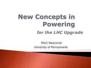
New Concepts in Powering for the LHC Upgrade Mitch Newcomer University of Pennsylvania
Trackers at the LHC ATLAS pixel detector services ATLAS Inner Det. Cables ATLAS SCT L. Gonella - ATLAS Upgrade Week - Apr. 2010 LHC Trackers wired in parallel. Use all available cross section for cabling Lose significant power as heat in cables. Vertex 2010
LHC ATLAS and CMS Silicon Trackers ATLAS SCT CMS Strips 6.2M channels 10M channels 3.5mW/ch 2.7mW 62m2 200m2 4088 Modules 15000 Modules ATLAS Inner Det. Material Distribution Mark Raymond ACES ‘09 Vertex 2010
SLHC Silicon Strip Trackers • ATLAS 6M Strips &300k Straws 42M Strips (150m2) • CMS (layout proposals just beginning) Silicon Analog RO Digital Silicon & multiple Tracking Layers • Higher Segmentation, more area More channels • Material Budget same or lower. • Cross Section for cabling nearly Constant • Re-use Services where possible • Total Power the same as LHC where possible Vertex 2010
Priorities for Upgraded Detector Power Services • Radiation Hardness ~1015n/cm2 , 50MRad • Low Mass • Small Additional Power dissipation • High Reliability > 10 year operation • Minimal Collateral loss due to failures. • Maximum Operability - low probability of false trip, easy, low overhead restoration of power. Vertex 2010
Powering • LHC - Parallel powering voltage and current nearly the same as powered unit • S LHC FEWER POWER CABLES/MODULE • Higher Primary Supply Voltage • Lower current in cables • Use the same or similar cables as LHC Lower fractional power loss in cables Smaller cross sectional area/module for services Power reduction realized by higher density ASIC technologies (130 or 90nm) will be realized in lower voltage, not current. (Digital Power= Cgate*V2). With more channels the current requirement may increase. Vertex 2010
Powering Concepts • Serial Power - One cable powers ‘n’ modules each with an equal current. ( est. 80% efficiency) • Vin = n*(Vmodule) • Constant Current = maximum current required by any module in chain + excess for modulation contingency. • Requires AC coupled Data & Control • Protection Shut down Short Module ( <100mV) • DC-DC - (V*I)in = (1/є)(V*I)Outє = efficiency • Vin optimized as a multiple of Vout based on tradeoffs between reduced cable cross section and technology and other constraints. (Est 80% efficiency) • Conventional DC Data & Control Protection Shut down = Open (no current) Much of the material for this talk taken from: The ATLAS – CMS Power Working Group Meeting March 2010 http://indico.cern.ch/conferenceDisplay.py?confId=85278 Vertex 2010
ATLAS Pixel OptimizationRegulators: on or off chip? Vertex 2010 L. Gonella - ATLAS Upgrade Week - Apr. 2010 • Answer depends on the ratio of converter/detector Figure of Merits (FOM) • Gives the radiation thickness penalty for using converters in active areas • FOM for silicon detectors: (load resistance) x (active area) • Of order of 10 Ω.cm2 for pixel and 100 Ω.cm2 for strip detectors • FOM for converters: ε/(1-ε) x (output resistance) x (rad. thickness) x (area) • Typical FOM of external converters are in the order of 1-5% RL.Ω.cm2 at 80% efficiency • This gives a penalty of 0.5% RL per layer for pixels and ~0.05% RL for strips • A penalty >0.2% RL per layer is regarded as too severe Only strips can use external converters Pixel detectors must use internal (on-chip regulators) which usually have a FOM of less than 0.5% RL.Ω.cm2 (just the external blocking capacities)
Module MC +nABCn Module MC +nABCn Module MC +nABCn Serial Power Module/Hybrid Current path Ihyb/module Vraw /I = Zmodule A Ihyb/module Variable Z Regulators Distributed over FEIC Regulated ASIC Voltages SHUNT ( ABC’s etc. ) . . . . B Vertex 2010
Serial Power Several possible approaches have been implemented: Available technology is sufficient for “at” scale prototyping. • Bonn - SHUNT–LDO for ATLAS Pixels • FNAL - SPI chip Self Contained Shunt ASIC • Penn – Distributed Shunt (through FEIC’s) • Krakow – SCT Shunt Load Shared and regulated in each ABCn. Fabbed in ABCn &Tested with SCT modules. Vertex 2010
ATLAS Pixels SP Shunt-LDO Zin > Zout Vin V-I characteristic of 2 Shunt-LDO in parallel @ different output voltages (MEASUREMENT RESULTS) Vout 1 Vout 2 Shunt – LDO Michael Koragonis Vertex 2010 L. Gonella - ATLAS Upgrade Week - Apr. 2010 • Combination of a LDO and a shunt transistor • Shunt transistor is part of the LDO load • LDO power transistor works as an input series resistor for the shunt • Advantages for Serial Power • Shunt-LDO regulators can be placed in parallel without problems regarding mismatch & shunt current distribution • Also, Shunt-LDO having different output voltages can be placed in parallel • Shunt-LDO can cope with an increased supply current if one FE-I4 does not contribute to the regulation • Working principle and good performance demonstrated with 2 prototypes already • Nominal Power Efficiency of 2 Shunt-LDO in parallel with different Vout = 75% (calc.)
FNAL SPI (Serial Powering Ic) Vertex 2010
Layout of SPI Chip Vertex 2010
SPI chip Tests Bump Bonds for High current Shunt SPI under test for CMS Pixels see talk of Aida Todri, FNAL at PWG 2010 meeting. Vertex 2010
ABCn ABCn ABCn ABCn ABCn ABCn ABCn ABCn ABCn ABCn ABCn ABCn ABCn ABCn ABCn ABCn ABCn ABCn ABCn ABCn ABCn ABCn ABCn ABCn SP Distributed ShuntModule/Hybrid for ATLAS SCT Power current path distributed among ABCn chips. No interruption. “Xtra material” OP amp & traces & Protection Vhybrid Vraw Ref Regulator OPAMP monitors Vraw Drop for whole module External feedback control loop sets Averagecurrent to desired value. Each FEIC participates in current shunting Heat load differences should be less than 2% chip to chip. Upgrade Workshop DESY 2010 Vertex 2010
SP Distributed shuntSome Advantages Ashley Grenall Default prototype power scheme • Existing Technology is sufficient. • Largest FEIC shunt Current 200mA. • Largest Power Diss ~50mW/FEIC • Many Amps reserve Regulation. • No Xtra Devices in Current Path • Impact on Material Budget Minimal. • No oscillators or RF components. • 200ns Response Time. • AC communications not difficult to • implement. • Simplicity. Vertex 2010
One Both Cntrl Lines 5 Amps Ashley Grenall Vertex 2010
Tony Affolder 0.5, 1.0, 1.5 fC Col 0 Initial measurement Col 1 Col 0 Col 1 Vertex 2010
ATLAS SCT Serial Power Protection Serial Powering near short across the module to shut it down. BNL designed a PCB based protection board using commercially available parts that offers both addressable power on/off and an autonomous shunt shut down. It will be used for testing with stavelets, 8 serially connected hybrids and stave 09, 24 hybrids.
SPP- Serial Power (control) & Protection ASIC • One chip solution using the same 130nm technology as FEIC’s. • Separate power ,compatible with ABCn 2.4V & ABC130 1V • Can satisfy radiation tolerance requirements. • Offers Serial Power regulation. • Autonomous fault detection and shut down. • Individual addressable power control “on” and “off”. • Single additional line on stave bus for power and PWM addressing. Vertex 2010
Serial Power & Protection ASIC 130nm DG transistors for 2.4V Analog and Digital logic on chip. ~ 6mA current draw ~15mW for the ASIC. Global Power & com( ~20V) Redundant Shunt Control ** “External FET gate” to accommodate Shutdown mode when used with ABCn Upgrade Workshop DESY 2010
SPICE sims of shutdown Fault condition 1.5A spike 200uS Zoom in 3uS Hybrid Current with 1.5A spike Hybrid Shut Down Signal Shunt Control 1.1V nom 1.3V Trigger Vhybrid 500ns 90mV OV comparator input Upgrade Workshop DESY 2010
DC-DC convertors • Yale - Commercial Devices including some success with Rad Tolerant devices, Inductor Design • CERN • RAD Hard custom ASIC Buck convertor • Switched Capacitor Convertors • EMI analysis and reduction • Miniatuized packages • AACHEN Study of EMI emission implementation of CERN AMIS2 ASIC for CMS Pixel DCDC convertor. Vertex 2010
DC – DC ATLAS SCT upgrade stave Optical link Building Blocks • Stage1: • Inductor-based buck • Vin = 10-12 V • Vout = 2.5-1.8 V • Pout = 2-4 W 10-12V Detector 2.5 V • Stage2: • On-chip switched capacitor • Vin = 2.5-1.8 V • Conversion ratio ½ or 2/3 • Iout = 20-100 mA GBT,Opto 1.25V Same blocks can be combined differently to meet custom system requirements 10-12V Stave Controller Intermediate voltage bus Proposed distribution scheme based on 2 conversion stages Example design shown for ATLAS short strip concept 10-12V F.Faccio – CERN/PH/ESE PWG meeting ‘10 Vertex 2010
DC – DC Stage 1 Commercial ASICs Maxim Buck Converter not Rad Hard SatishDiwhan Enpirion OK Except for Internal Inductor Efficiency ~ 70% @ 4A Design by SatishDiwhan, Yale Vertex 2010
CERN WP2: On-detector power distribution • ATLAS, CMS and “common” Working Groups on powering are an efficient communication and coordination tool • We contribute regularly to the meetings with large number of talks • Direct collaboration with ATLAS and CMS • CMS tracker • Work in parallel on DCDC boards done in RWTH and CERN, with regular exchanges of results. We provide ASICs and our knowledge on board layout, converter functionality, filtering and shielding issues • Our results and contribution were fundamental to drive the choice of the CMS task force that selected DCDC option for powering their upgraded tracker • Our standardized test setup to measure conducted noise was cloned in other Institutes participating in CMS (we helped with information and documentation) • We will provide the IP block of the ½ converter based on switched capacitors • ATLAS tracker • Characterization of prototype hybrids powered with DCDC converters is done in collaboration with Liverpool and Geneva Universities • We participate in the definition of the power distribution in the prototype supermodule developed at KEK and Geneva University. We collaborate with Liverpool University for integration of DCDC converters in the prototype stave developed in the UK-US • Design of an on-chip ½ converter based on switched capacitors in collaboration with AGH Cracow • Direct expressions of interest for the converter (other than silicon strip detectors for phase2) • CMS pixel detector for phase1 upgrade (PSI, RWTH, Fermilab) • CMS HCAL for phase1 upgrade (Minnesota, Fermilab, ….) • ATLAS TileCal (Argonne Nat. Labs) F.Faccio – CERN/PH/ESE
CERN Buck converter ASIC: prototypes fabbed to date Stage 1 DC-DC Step down going from 12-15V down to ~2.5V F.Faccio – CERN/PH/ESE
IHP2 prototype • Second prototype in the IHP SGB25VGOD technology • Design included in MPW run of Jan10 Expected back in May 2010 • Additional features integrated in the prototype: • Linear regulators • Bandgap • Overcurrent protection • Improvement in the adaptive logic • Triplication and logic against SEU • Enablers • Complete circuit • Over current protection • Dimension of the power transistors • External components needed • Compensation network 2.9mm 3mm S.Michelis CERN/PH
Prototype for SCT Hybrid now • The AMIS2-PIB can deliver 3.5A : insufficient for the ABCn hybrid. • A compatible DCDC, with same geometry and connector has been designed using a commercially available controller. • Results from first prototype: • Switches at 3 MHz, delivering 5A. • Can power one full hybrid. • Efficiency reaches 87% at 2A, and is around 80% at 4A. • Output stable up to 5A load. G. Blanchot, PH/ESE Vertex 2010
UniGe Module Position of hybrids Conducted noise test Measurements performed with the help of Sergio Gonzalez from University of Geneva. Radiated noise at corner DC – DC works on ABCn Prototype module! Reference noise: ENC Average: 560 ENC Sigma: 32 Radiated noise on top of hybrid Vertex 2010 G. Blanchot, PH/ESE
PWG ‘10 Vertex 2010
PWG ‘10 Vertex 2010
DC – DC (stage 2) CERN submission in 130nm CMOS June 2010 Primary Designer Michal Bochenek Vertex 2010
DC – DC Advantages • Highly Developed by Commercial Vendors • No requirement for constant current draw. • Conventional DC data/control communications. Development Initiatives • CERN WP2 priority development • Several groups pursuit of low mass, low EMI inductor designs. Vertex 2010
Welcome System Test Set-Up • Two DC-DC converters per module • Integrated via additional adapter • Vinfromlab power supply TEC petal • APV25 readoutchip: • 0.25 µm CMOS • 128 channels • - analoguereadout • - per channel: pre-amp., CR-RC shaper, pipeline • - = 50ns • - 1.25V & 2.50V supply • - I250 = 0.12A, I125 = 0.06A Ring 6 modules 6.4 6.3 6.2 6.1 Motherboard Jan Sammet
Welcome Effect of 30µm Aluminium Shielding BZ-Field of AMIS2-V1, Vin=8.5V, Vout=2.5V, f=1.3MHz, L=600nH No shielding Inductor only PCB only Complete converter • Shielding only the inductor is not sufficient • B-field not measurable when converter is completely encased Jan Sammet
Conclusions Two Powering Approaches appear to be working both are projected to have similar efficiency Serial Power - Basic Pros - Lower Material, DC operation Basic Cons - Modularity inconveniences AC coupling DC-DC - Basic Pros - no modularity constraints, conventional DC signaling. Basic Cons - Two elements in current path Technically challenging for remote high rad environment. Lots of excellent work in progress. Vertex 2010