Download
1 / 12
120 likes | 312 Views
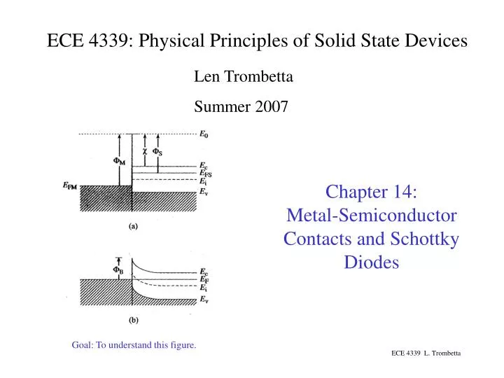
ECE 4339: Physical Principles of Solid State Devices. Len Trombetta Summer 2007. Chapter 14: Metal-Semiconductor Contacts and Schottky Diodes. Goal: To understand this figure.

E N D
ECE 4339: Physical Principles of Solid State Devices Len Trombetta Summer 2007 Chapter 14: Metal-Semiconductor Contacts and Schottky Diodes Goal: To understand this figure. ECE 4339 L. Trombetta
The energy needed to get an electron from the bottom of the conduction band to the vacuum level Eo is the “electron affinity”, c. FM is the metal workfunction (recall the photoelectric effect). FS is the semiconductor workfunction. It depends on c as well as the doping density. ECE 4339 L. Trombetta
M-S Contact Electrostatics ECE 4339 L. Trombetta
E electric field V(x) FB “flat bands” The charge density and hence the solution to Poisson’s equation is the same as for a one-sided p-n junction. ECE 4339 L. Trombetta
W W W Equilibrium: We have set xn = W. Applied bias VA: ECE 4339 L. Trombetta
The energy band diagram, electric field, and potential in the M-S (n-type) junction are similar to that in a p+n junction, but the current components are different. The Schottky diode is a majority carrier device: majority carriers are mostly responsible for current flow. In the M-S junction, electron emission over the barrier (thermionic emission) is dominant. Diffusion and drift current, which are important in pn junctions, are negligible here. ECE 4339 L. Trombetta
Thermionic Emission This comes from statistical mechanics… ECE 4339 L. Trombetta
M-S Contact I-V R-G and diffusion current components are much smaller here than in pn junction devices. is Richardson’s Constant ECE 4339 L. Trombetta
Schottky-Clamped BJT Since the Schottky “on” voltage is a little smaller than for a pn junction, the BC junction forward bias is limited. During saturation, this limits the number of minority carrier in the base, and improves device speed. ECE 4339 L. Trombetta
We can form on Ohmic contact between a semiconductor and a metal by heavily doping the region just below the metal. ECE 4339 L. Trombetta