Download
1 / 41
410 likes | 604 Views
Flyura Djurabekova. Atomistic approach in simulations of electrical breakdowns on metal surfaces. ISDEIV: International symposium on Discharges and Electrical insulation in Vacuum in Tomsk, Sept. 2012 . Helsinki Institute of Physics and Department of Physics University of Helsinki Finland.

E N D
Flyura Djurabekova Atomistic approach in simulations of electrical breakdowns on metal surfaces ISDEIV: International symposium on Discharges and Electrical insulation in Vacuum in Tomsk, Sept. 2012 Helsinki Institute of Physics and Department of Physics University of Helsinki Finland
University of Helsinki, Finland Behind the model… Doc. Flyura Djurabekova Senior scientist M Sc AarnePohjonen Dislocations Prof. Kai Nordlund M Sc AvazRuzibaevCharges on surfaces M Sc Stefan Parviainen Field emisssion and neutral atom evaporation Dr JuhaSamela Sputtering and cratering Dr LottaMether Plasma simulations CERN, Switzerland Dr.Helga TimkoPlasma simulations (CERN, Switzerland) Dr. VahurZadin FEM calculations, Tartu Univ. Ms. RiikkaRuuth Surface damage Inspiration comes from CERN, Geneva Dr. Walter Wuensch Sergio Calatroni
Outline • Multiscale model to approach the problem of electrical breakdown • Surface charge • Dislocations as a media of surface response to electric fields • Electric discharges near a metal surface • Summary Accelerator Laborary, Helsinki
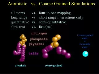
Tools in use: • In our group we use all main atomic-level simulation methods: • Density functional theory (DFT) • Solving Schrödinger equation to get electronic structure of atomic system • Molecular dynamics (MD) • Simulation of atom motion, classically and by DFT • Kinetic Monte Carlo (KMC) • Simulation of atom or defect migration in time • Simulations of plasma-wall interactions • Simulation of plasma particle interactions with surfaces • We use all of them to tackle the arcing effects!
Multiscale model to simulate electrical breakdown BukhardJüttner1979 Stage 1:Charge distribution @ surface Method:DFT with external electric field ~few fs Stage 2: Atomic motion & evaporation + Joule heating (electron dynamics) Method: Hybrid ED&MD model (includes Laplace and heat equation solutions) ~few ns ~ sec/min ~ sec/hours Stage 3a: Onset of tip growth; Dislocation mechanism Method:MD, FEM Stage 3b:Surface evolution: taking into account all the studied dynamic processes (including electromigration) Method:Kinetic Monte Carlo Stage 4:Plasma evolution, burning of arc Method:Particle-in-Cell (PIC) ~10s ns ~100s ns Stage 5: Surface damage due to the intense ion bombardment from plasma Method:Arc MD
Workfunctionnear an adatom in Cu • We have calculated the work function for Cu surface when a single adatom is present WS EV
Solution of 3d Laplace equation for the surface with the tip of 20 atomic layers, mixed boundary condition (Dirichlet at bottom, Neumann at top) (colors on atoms represents the charges, details in Stefan Parviainen’s talk)
Evolution of a tip placed on Cu surface • We developed a novel approach to follow the dynamic evolution of partial charge on surface atoms by combining the MD and classical ED (solving Laplace equation) • The dynamics of atom charges follows the shape of electric field distortion on tips on the surface • Temperature on the surface tips is sufficient => atom evaporation enhanced by the field can supply neutrals to build up the plasma densities above surface. Details in F. Djurabekova, S. Parviainen, A. Pohjonen and K. Nordlund, PRE 83, 026704 (2011).
DFT calculations to validate the charges on surface atoms • DFT details: • Code: SIESTA • For exchange and correlations functionals the Perdew, Burke and Ernzerhof scheme of Generalized gradient approximation (GGA) • Slab organized in 8 layers+ 8 layers of vacuum • External field is added to calculate the electrostatic potential in the vacuum Eo=-1 GV/m
Je Fowler-Nordheim approximation for field emission • Every atomic column produces the current dependent on the field above the column. The current from the tip is an average over all the columns. E0 Ei Fowler-Nordheim constants: No electromigration is still taken into account!
The heat conduction from the tip has been implemented into MD • The heat conduction from the tip has been implemented into PARCAS by solving the heat conduction equation T, K T, K Here CVvolumetric heat capacity. Phonons are implicitly present in classical MD. In the equation we include only electron thermal conductivity given by the Wiedemann-Franz law Jel(x) J(x) Electric current (resistive heating) Where Lorenz number is found as Lattice and electronic heat conduction S. Parviainen, F. Djurabekova, H. Timko, and K. Nordlund, Comput. Mater. Sci. 50, 2075 (2011).
+ + + + + + + + Stresses due to the field • The main agreement in the field is that the rapid releasing of microstresses, which is generally present on grain boundaries and can be enhanced by any external agents as mechanical treatment or T-cycling, the migration of defect complexes is stimulated. • The strain by the huge electric field can cause the dislocation motion and redistribution of the microstress. → E STRESS =0E2/Y
What are the field emitters? Why do we look for dislocations? • The dislocation motion is strongly bound to the atomic structure of metals. In FCC (face-centered cubic) the dislocation are the most mobile and HCP (hexagonal close-packed) are the hardest for dislocation mobility. A. Descoeudres, F. Djurabekova, and K. Nordlund, DC Breakdownexperimentswith cobaltelectrodes, CLIC-Note XXX, 1 (2010).
Voids∀precipitates: lattice irregularities are probable source of a protrusion growth • We simulated a void near {110} Cu surface , when the high tensile stress is applied on the surface. Bottom is fixed, lateral boundary allowed to move in z direction. A. Pohjonen, F. Djurabekova, et al., Dislocation nucleation from near surface void under static tensile stress on surface in Cu, Jour. Appl. Phys. 110, 023509 (2011).
Concurrent ED-MD simulations of dislocations on a near-surfacevoid • Half-void of diameter 4nm in {110} Cu surface. (N of atoms 170000 atoms…) • E0=22 GV/m (exaggeration is required to simulate the dislocation within the MD time span) • T = 600 K
Back to reality We also performed the series of FEM calculations. We obtained an interesting result: The presence of surface near to the void increases the chances for dislocation nucleation, but not drastically! • SEM images courtesy of Dr. Tomoko Muranaka (Uppsala Univ.)
FEM calculations of the void on stainlesssteel • The Finite Element Method calculations were done for steel due to the availability of all the parameters needed for elastic deformation and yield strength. (the isotropic tangent modulus in hardening model are not yet confirmed from other sources) • Calculation of the electric field as a function of the height of the protrusion • Different scales correspond to the depth where the void is buried
Dislocation-based model for electric field dependence • Now to test the relevance of this, we fit the experimental data • The result is: Stress model fit Power law fit [W. Wuensch, public presentation at the CTF3, available online at http://indico.cern.ch/conferenceDisplay.py?confId=8831.] with the model.]
Temperaturedependence of BPP • Experimental data on dependence of breakdown rate on the peak temperature increase in accelerating components K. Nordlund and F. Djurabekova, Defect model for the dependence of breakdown rate on external electric fields, Phys. Rev. ST-AB 15, 071002 (2012).
jFE Plasma evolution Corresponding to experiment... • Up to now we have • electrostatic PIC-MCC codes: • 1d3v • 2D-model • Provide us with a link between • Micro- & macroscopic surface processes: Triggering (nano-scale) plasma crater formation (visible effect) • Theory & experiments: Using reasonable physical assumptions (theory), the aim is to predict the evolution of measurable quantities (experiment) H. Timko, K. Matyash, R. Schneider, F. Djurabekova, K. Nordlund, A. Hansen, A. Descoeudres, J. Kovermann, A. Grudiev, W. Wuensch, S. Calatroni, and M. Taborelli , Contrib. Plasma Phys. 51, 5-21 (2011)
Particle-in-Cell plasma simulation • The 1D PIC simulations give the plasma density time evolution above the surface:
1D PIC code • There is a sheath potential drop present (∼ 200 eV, corresponding to an electron temperature of ∼ 40 eV), however, it is difficult to notice it on the scale.
Cathode damage due to ion bombardment • Knowing flux & energy distribution of incident ions, erosion and sputtering we can simulate the surface damage with MD
MD simulations of surface bombardment on a given area A Ion flux and energy distribution corresponded exactly to that from PIC simulations! Flux of ~1025 on eg. r=15 nm circle =>one ion/20 fs!! Multiscale modelling of sparks:Classical MD simulations Top view Side view
Surface damage due to plasma • Previously we simulated only the surface, which was held at ambient (room) temperature. The plasma-surface interaction was simulated as (i) thermal heating and (ii) plasma ion bombardment (“shower”) with the energy ~ 6 keV, 100 ions over 30 nm spot; flux of ~1025 ions/sec.
Analysis of surfacedamage • Comparing arc plasma bombardment and thermal heating, we found that: • Enhanced sputtering yield above a threshold, corresp. to the melting point • Only for plasma bombardment: (i) heat spike & cluster emission above the threshold (ii) experimentally seen complex crater shapes can form • Sputtering as the function of depositedenergy threshold
Plasma-surface interaction.Crater formation. SEM AFM simulation
Comparison to experiment • Self-similarity: Crater depth to width ratio remains constant over several orders of magnitude, and is the same for experiment and simulation 10 μm 50 nm H. Timko, F. Djurabekova et al., Mechanism of surface modification from the arc plasma-surface interaction in Cu, Phys. Rev. B 81, 184109 (2010).
Plasma impacts on Cusurface • Now we have simulated a number of plasma impacts on the surface with different surface temperatures and different regimes of cooling • We simulated three types of surfaces: • Molten at Tm • Molten, just below Tm temperature (undercooled liquid) • Still crystal, just below Tm temperature (overheated crystal) • Flux=4.9 x 1024 ions/cm2/s • Energy E=6 keV
Moltensurfacebombardedwith 100 ions, 200ions, 500 ions, 700 ions
Molten surface: 100 ions • Surface is preheated to the melting temperature. Electronic conduction takes the temperature away during the bombardment. Cooling is done via so called electron-phonon coupling model, applied widely in the field of ion irradiation of metals
Undercooledliquidsurface • At first we raised the temperature to the melting point, queched it just below the melting point
Overheatedcrystal • The temperature is just below the melting point, but the crystal structure is preserved. The efficiency of temperature removing from the system in the case to the right is twice more efficient.
Overheated crystal surface • The same results with the profile view. The surface to the right quenched faster.
Finalcratersize as a function of fluence • Increase of the bombardment time deepens the craters, but if the bombarded surface is molten fully the crater stays shallow
Summary • We develop a multiscale model, which comprises the different physical processes (nature and time wise) probable right before, during and after an electrical breakdown event: • All the parts of the general model are pursued in parallel. We develop intense activities to cover all possible aspects. • Our modeling shows: • Plasma is fed from the tips grown under the high electric field • Tip growth can be explained by the relaxation of stresses inside of a material by the dislocation motion • A dislocation-mediated mechanism can explain the high slopes of breakdown rates against the accelerating fields
TOPIC A: BREAKDOWN AND FLASHOVER • A1. Vacuum breakdown and pre-breakdown phenomena • A2. Surface discharges and flashover phenomena • A4. High field effects in microelectromechanical systems and nano-structures • TOPIC B: VACUUM ARCS • B1. Switching in vacuum and related phenomena • B2. Interaction of vacuum arc with magnetic field • TOPIC B: VACUUM ARCS • B3. Vacuum arc physics • B4. Computer modeling and computer aided design • B5. Pulse power physics and technology • TOPIC C: APPLICATIONS • C1. Vacuum interrupters and their applications • C2. Deposition of coatings by vacuum arc plasmas and related technologies • C3. Electron, ion, neutron, X-ray and other beam and light sources • C4. Accelerators and fusion reactor related issues • C5. Space related technologies
Possibleenhancement of currentflowthrough the gap • By Kai Hencken, ABB Switzerland Ltd. They studied the possible ways how the current flow can be enhanced. With the MC simulation code PENELOPE they analyzed the production of both x-rays and secondary electrons for gap voltages between 12 and 42 kV. The study showed the effect is negligible! “Backscattered electrons enhance the x-ray photon yield. But the total number of photons produced and also the number of secondary electrons released from the cathode remains small. Their total yield in comparison with the number of primary electrons is rather small. We therefore conclude that x-ray photons play only a minor role in explaining the pre-breakdown current flowing through the gap in vacuum interrupters.”
Field emission alonedoesnotexplain the origin of breakdown! • The group from Schneider Electric showed that only the mechanism of electron field emission alone could not explain the breakdown in vacuum at the origin of late breakdown phenomena. • CuCr75/25, inrush current 20 kA (FEE current was measured after interrupting this current),