Download
1 / 60

E N D
Electron transport through superconducting weak links can be understood in terms of Andreev bound states. They originate from conduction channels with each conduction channel giving rise to two Andreev bound states. In order to get access to single Andreev bound states we have used a system with a few conduction channels at most – quantum point contact. We have studied supercurrent across such a phase-biased atomic size contacts. For broad phase interval around p we have found suppresion of supercurrent – effect attributed to quasiparticle trapping in one of the discrete subgap Andreev bound states formed at the contact. Since single Andreev bound state can sustain supercurrent up to 50nA, such a trapping has a sound influence on the response of the atomic contact. Next to single Cooper-pair devices in which parity of the total number of electrons matters, it is another demonstration of a situation, when a single quasiparticle leaves a macroscopic trace. However, unlike a single Cooper device, atomic contact contains no island at all. The trapped quasiparticles are long-lived, with lifetimes up to hundreds of ms. Trapping occurs essentially when the Andreev energy is smaller than half the superconducting gap D. The origin of this sharp energy threshold is presently not understood. PRL ,106, 257003 (2011) ABSTRACTQuasiparticle Trapping in Andreev Bound StatesMaciejZgirski*, L. Bretheau, Q. Le Masne, H. Pothier, C. Urbina, D. EsteveQuantronics Group, SPEC, CEA Saclay, France*presently: Institute of Physics, PAN, Warsaw
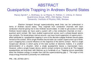
Quasiparticle Trapping in Andreev Bound StatesMaciejZgirski*, L. Bretheau, Q. Le Masne, H. Pothier, C. Urbina, D. EsteveQuantronics Group, SPEC, CEA Saclay, France*presently: Institute of Physics, PAN, Warsaw L. Bretheau Q. Le Masne H. Pothier D. Esteve C. Urbina PRL ,106, 257003 (2011)
MOTIVATION E(d) S I S +D +EA 0 d -EA -D • Josephson effect in superconducting weak links – unified approach • Spectroscopy of Andreev Levels • Andreev Qubit t S S
ANDREEV REFLECTION COUPLING OF eh AND h$ N-S interface S N
PHASE-BIASED SHORT, Ballistic SINGLE CHANNEL L < x t =1 fL fR Fabry-Perot resonator
Andreev spectrum E +D 0 E(d) +D -D E→ 2 resonances 0 d p 2p E← -D ANDREEV BOUND STATES in a short ballistic channel (t=1 ) t = 1 fL fR
E(d) E +D +EA +D 0 d -EA -D 0 -D ANDREEV BOUND STATES in a short reflective channel (t <1 ) Andreev spectrum t < 1 Furusaki, Tsukada C.W.J. Beenakker (1991) Central prediction of the mesoscopic theory of the Josephson effect
SUPERCONDUCTING WEAK LINKS S I S Weak link = ensamble of independent transmitting channels, each characterized by transmission t (Landauer picture) N – number of transmission channels t - transmission Atomic contact: N ~ 1 0 < t < 1 Tunnel junction: Ninfinity t ->0 g = gL - gR Current phase-relation Iac(d) = ? t S S
E(d) +D +EA 0 d -EA -D FROM ANDREEV BOUND STATES TO SUPERCURRENT Ground state : Current-phase relation
Current – phase relation… E(d) +D 0 d -D …is a probe of a configuration of Andreev bound states
Towards ANDREEV QUBITS E(d) +D +EA 0 d -EA -D Use even states Use quasiparticle (spin ½) states Zazunov, Shumeiko,Bratus’, Lantz and Wendin, PRL (2003) Chtchelkatchev and Nazarov, PRL (2003)
ATOMIC CONTACT = SIMPLEST WEAK LINKfabrication & characterization I V S S • 1 atom contact = few conduction channels (Al: 3) • Stable system • Can becompletelycharacterized
MICROFABRICATED BREAK-JUNCTIONS metallic film pushing rods Flexible substrate insulating layer counter- support
PIN code of the atomic contact Scheer et al. PRL 1997
Atomic Squid… IAC V or
measurement OPEN …allows to determine channels transmissions… V I Ib transmissions {ti}
measurement SHORT …and impose phase on atomic contact g Ib IJJ>> IAC “Strength” of the weak link ~ critical current
Switching of the Atomic Squid Ib switching IAC V retrapping or g d
SWITCHING MEASUREMENTS Ib (nA) Supercurrent branch <Isw> V (µV) « s curve » Ib Pulse height P tp Tr time N Switching probability V time Ib (nA) n Tr=20µs tp=1µs N=5000 usually
Flux Modulation pattern for ATOMIC SQUID= I(d) of the atomic contact When SQUID switches, phase across JJ is approx. the same independently of applied magnetic flux => interference pattern is current-phase relation of atomic contact The ground Andreev state is well-known… I0-switching current of junction alone Theses in Quantronics: M. Chauvin, B. Huard, Q. Le Masne Della Rocca et al., PRL 2007
Switching probability map with normal leads P (Ib,j) P 1 P = 1 A vertical cut is an s-curve s = Ib/I0 I0 - critical current of JJ alone P = 0 0
Sample design bias line e-beam lithography designed to be 50W at T < 1K antenna
Switching probability map with superconducting electrodes T=40mK, Period= 20µs t={0.95, 0.445, 0.097} tp Tr time N j1 j2 Height of plateau is period dependent => some relaxation going on in the system
Switching curve with prepulse {0.95, 0.45 , 0.10} Erase memoryof the previous historybefore each measurement: P1(Ib) pP1(Ib)+(1-p)P2(Ib) ~ 0.1µs 1ms P2(Ib) 1.3 {0.45 , 0.10} 1 delay « prepulse » 0 After switching, system is where we expect it to be with probability p
Blocking the most transmitting channel {0.45 , 0.10} {0.95 , 0.45 , 0.10}
E(d) +D 0 d -D QUASIPARTICLES IN A SUPERCONDUCTING POINT CONTACT E EA D -EA 0 -D 2 qps Ground state 1-qp states
Excitation picture The smallest excitation breaking parity = one unpaired quasiparticle All electrons paired Excited Cooper pair
Two scenarios Initial state QP 1. Weight = p nQP nQP Channel switched on 2. Weight = 1 - p E E Channel switched off Switching probability is the weighted average of these 2 scenarios.
Modulation curves on different contacts {1,0.072,0.072} AC1 {0.998,0.56,0.124} AC2 {1,0.7,0.24,0.24,0.06} AC3 The most transmitting channel is sometimes switched off
1QP STATE RELAXATION MEASUREMENTS Flux line Phase across contact d jw ji Current line di Ib 0 waiting time TR(d) Pinf(d)
A few 100ms relaxation time {1,0.07,0.07} -0.6p 0 0.6p T=29mK d phase across atomic contact Symmetryaroundp Monotonousbehaviour
Relaxation as a function of phase across Atomic Contact for different transmissions T=29mK
Energy threshold for relaxation E(d) +D 0 p 2p d -D E- Relaxation instantaneous only forAndreev Bound states with energies bigger than 0.5 D ~25GHz ~1K
Energy threshold for relaxation nQP nQP D D/2 WHY? E E
Possible explanation hn hn ~ D/2 nQP nQP D D/2 E E
Conclusions • Atomic contacts with tunable transmissions • Atomic Squid to measure current-phase relation of atomic contact with switching measurements - for ground Andreev bound states excellent agreement with theory • Quasiparticle poisoning => disappearence of the most transmitting channel; • long relaxation for Andreev Cooper pair binding energies smaller than 0.5D, sharp cut off for binding energies bigger than 0.5D (?) • Dispersive measurements of resonant frequency of resonator + atomic squid • Trials to observe avoided level crossing (atomic contact embedded in resonator) • No evidence of excited Andreev state in 2 different experiments (switching measurements, coupling to resonator ) • Current Status: Josephson Junction spectroscopy of Atomic Squid – observed avoided level crossing • PLASMA FREQUENCY – ANDREEV GAP
Temperaturedependence {1,0.07,0.07}
Does excited Andreev state exist? (OPTIONAL)
Sample design bias line e-beam lithography designed to be 50W at T < 1K antenna
Capacitor + inductive lines Andreevmon (or Andreevnium) 10µm gap Capacitor C = 60 pF 140µm 680µm inductive lines, 900nm wide, 70 + 54 nm thick Al Ltotal = 1.8nH antenna (5µm wide short of CPW)
Electromagnetic environment is important IB R d g L RF line VB bias line
Trials to observe excited Andreev state Peak position isfrequency-dependent Expected I 0 0.5 1 d / 2p
Andreev Qubit in cavity Weak coupling
Cavity Quantum Electrodynamics VAC in VAC out strong coupling regime
Let 2 level system interact with resonator Andreev Gap Bare Resonator eigenfrequency Red – expected position of resonance Interaction “off” Interaction “on” avoided level crossing Coherent exchange of energy between resonator and artificial atom
2 CHANNELS POISONING {0.95, 0.94, 0.60, 0.34, 0.30, 0.29, 0.27, 0.26, 0.24, 0.2}
Pollution of 2 channels {0.957, 0.948, 0.601, 0.344, 0.295, 0.291, 0.27, 0.262, 0.242, 0.2} 1 channel blocked 2 channels blocked All channels