Download
1 / 33
440 likes | 1.07k Views
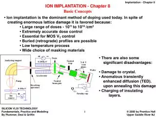
Chapter 8 Ion implantation. Introduction and application. Ion implantation tools. Dopant distribution profile. Mask thickness and lateral distribution. Effect of channeling. Modeling: nuclear and electronic stopping. Damage caused by ion implantation. Damage repair.

E N D
Chapter 8 Ion implantation Introduction and application. Ion implantation tools. Dopant distribution profile. Mask thickness and lateral distribution. Effect of channeling. Modeling: nuclear and electronic stopping. Damage caused by ion implantation. Damage repair. NE 343: Microfabrication and thin film technology Instructor: Bo Cui, ECE, University of Waterloo; http://ece.uwaterloo.ca/~bcui/ Textbook: Silicon VLSI Technology by Plummer, Deal and Griffin
Looking at Si at different orientations 110 111 Random tilt and rotation 100
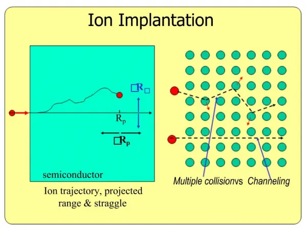
Si Si Si Si Si Si Si Si Si Si Si Si Si Si Si Si Channeling effect • Occur when ion velocity is parallel to a major crystal orientation. • Some ions may travel considerable distances with little energy loss. • Once in a channel, ion will continue in that direction, making many glancing internal collisions that are nearly elastic (their stopping is then dominated by electronic drag only), until it comes to rest or finally dechannels. The latter may be result of a crystal defect or impurity.
Channeling effect: critical angle Critical Angle: defined as the maximum angle between the ion and the channel for a glancing collision to occur. Where Z1 is the incident ion atomic number, Z2 is the target atom atomic number, E is the acceleration energy in keV (voltage), and d is the atomic spacing in the direction of the ion path in angstroms. Note: channeling is more likely for heavy ions and lower energies. But another source says the opposite: The effect is particularly pronounced when implanting light atoms on axis into a heavy matrix sine the ion’s atomic radius is much less than the crystal spacing.
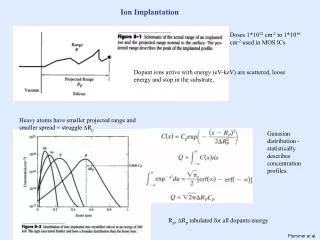
Impurity distribution due to channeling effect Even (the complicated) Pearson profile fails in the case of crystalline silicon where ion channeling may occur. The resultant profile can be described by a “Dual-Pearson” distribution. Phosphorus impurity profiles for 40keV ion implantations to silicon at various angles from the <110> axis. long “tail”
Si Si Si Si Si Si Si Si Si Si Si Si Si Si Si Si Methods to reduce channeling effect Most IC implantation is done off axis. A typical tilt angle is 7o. A thin screen oxide which is amorphous is often used, causing some randomization of incident beam before it enters the lattice.
Methods to reduce channeling effect Destroy the lattice before implantation • High dose Si+ implantation to convert the surface layer into amorphous Si. • Implantation of desired dopant
Chapter 8 Ion implantation Introduction and application. Ion implantation tools. Dopant distribution profile. Mask thickness and lateral distribution. Effect of channeling. Modeling: nuclear and electronic stopping. Damage caused by ion implantation. Damage repair. NE 343: Microfabrication and Thin Film Technology Instructor: Bo Cui, ECE, University of Waterloo, bcui@uwaterloo.ca Textbook: Silicon VLSI Technology by Plummer, Deal, Griffin
Ion – substrate interaction The ions are stopped at random positions, mostly not in crystalline sites, so not active as dopant (need anneal to active them).
Ion implantation energy loss mechanisms LSS theory: in 1963, Lindhard, Scharff and Schiott proposed that the energy loss of incident ion can be divided into two independent process, namely nuclear stopping and electronic stopping. Total energy loss is the sum of the two processes. Nuclear stopping, crystalline Si substrate damaged by collision. Electronic stopping, electronic excitation creates heat.
Nuclear and electronic stopping power Energy loss rate (N is target atom density) Nuclear stopping power (unit: eV cm2) Electronic stopping power Ion range Light ions/at higher energy: more electronic stopping Heavier ions/at lower energy: more nuclear stopping H+: electronic stopping dominates B+: electronic stopping dominates As+: nuclear stopping dominates
Nuclear stopping power: Coulomb scattering (assume elastic) Incident ion interacts with nucleus of stationary ion. b = impact parameter The angles depend on masses and on b. Maximum energy loss: is when b = 0, = 0: To first order approximation:
Nuclear stopping power: Coulomb scattering (assume elastic) At 100keV and for Z=15, ion velocity ≈ 106 m/s! 1000 faster than speed of sound in solids. So ion is far past nucleus before nucleus can displace in response to Coulomb force. As fast particle have less interaction time with the scattering nucleus, the nuclear energy loss is small at very high energies/velocity. Thus the nuclear energy loss tends to dominant towards the end of the range when ion has lost much of its energy and where nuclear collisions produced most of the damage. Light ion slowed down at the end of range Heavy ion is slow (v M-1/2), more loss There are also inelastic collisions that transfer energy.
Electronic stopping power: also Coulomb interactions, but inelastic Non-local: ion experiences drag due to “free” or polarizable electrons. Local: passing ion causes internal electronic transitions => energy and moment transfer Because electrons can follow fields up to optical frequencies (velocities of 105 m/s - 100 times faster than phonons), electronic losses dominate at higher ion velocities. incident ion attracts electron polarization ion velocity => charge separation, drag
Electronic stopping power Drag force exerted on a moving ion in a dielectric medium, ion moves in same direction Charge and momentum exchange due to local electronic interaction, ion changes direction • A great deal of space in crystal is made up of the electron clouds from the atoms, many of these interactions will occur. • Even if the electron is not in the path of the ion, energy may be transferred through coulomb interaction. • Mass ratio between ion and electron is of order 105, so any single electron ion interaction will not dramatically alter the momentum of the incident ion.
Electronic and nuclear stopping power: summary Electronic collisions dominate at high energies. Nuclear collisions dominate at low energies.
Electronic and nuclear stopping power E2: energy where electronic stopping power is equal to nuclear stopping power.
Electronic and nuclear stopping power B+: light, electronic stopping dominates As+: heavy, nuclear stopping dominates
Chapter 8 Ion implantation Introduction and application. Ion implantation tools. Dopant distribution profile. Mask thickness and lateral distribution. Effect of channeling. Modeling: nuclear and electronic stopping. Damage caused by ion implantation. Damage repair. NE 343: Microfabrication and Thin Film Technology Instructor: Bo Cui, ECE, University of Waterloo, bcui@uwaterloo.ca Textbook: Silicon VLSI Technology by Plummer, Deal, Griffin
Damage at end of range (EOR) The main disadvantage of ion implantation is the production of lattice damage (vacancies and interstitials, or V/I) which may evolve from simple point defects into complex dislocations or voids. Eventually, implantation leads to an amorphous silicon structure (can be used for channeling reduction). Most damage can be repaired by annealing. However, annealing cycles of 30 min at close to 1000oC can cause considerable spreading of the implant by diffusion. EOR damage
Damage to the lattice: target atom displacement Energetic incident ions collide with target atoms, leading to their displacement. The result is an interstitial atom and a vacancy, V-I pair = Frankel defect. The displaced atoms may have energy high enough to further displace other target atoms along its path. (Si)SiSiI+ SiV I: interstitial; V: vacancy Vacancy Self interstitial
Number of displaced target atoms • An implanted ion can increase the number of recoil atoms only if it possesses an energy greater than 2Ed, where Ed is the minimum energy required to break four covalent bonds and dislodge a lattice atom. Ed is called threshold energy or displacement energy (for Si, Ed15eV). • When the energy of the incident ion or secondary knocked-on atom reach Ed, they can be considered stopped, because if they do damage to transfer all their energy to a lattice atom, they can cause a single displacement but remain at rest in the lattice position themselves. • Thus the number of displaced atoms created by an energetic particle can be estimated by N=En/2Ed, where En is the energy lost in nuclear collision. • For example, 30keV As ion will lead to roughly30000/(215)=1000 displaced atoms. • The number will be less for 30keV light ions, whose energy is mainly lost by electronic stopping.
Amorphization Critical dose • If the dose is high enough, the implanted layer will become amorphous. • The dose required to produce an amorphous silicon layer is called critical implant dose. • The heavier the impurity, the lower the dose that is required to create an amorphous layer.
Damage distribution Most damage is done by nuclear interactions (nuclear stopping) More crystalline damage at end of range, Sn > Se Less crystalline damage, Sn < Se
Damage distribution For light ion (lighter than target), small energy transfer to target atom for each collision, generate few displaced target atoms, and ion scatted at large angle. Low density non-overlapping damage, but over large area with a saw-tooth shape. For heavy ion, large energy transfer for each collision, small scatter angle. The displaced atom can further displace other target atoms. Small range, large damage density over small volume.
Chapter 8 Ion implantation Introduction and application. Ion implantation tools. Dopant distribution profile. Mask thickness and lateral distribution. Effect of channeling. Modeling: nuclear and electronic stopping. Damage caused by ion implantation. Damage repair. NE 343: Microfabrication and Thin Film Technology Instructor: Bo Cui, ECE, University of Waterloo, bcui@uwaterloo.ca Textbook: Silicon VLSI Technology by Plummer, Deal, Griffin
Annealing repair damage and activate dopants After implantation, we need an annealing step, usually under Ar, N2 or vacuum. A typical 900oC, 30min will: Restore silicon lattice to its perfect crystalline state - silicon atoms can move back into lattice sites at these temperatures. Put dopants into Si substitution sites for electrical activation - nearly all of the implanted dose becomes electrically active except for impurity concentrations exceeding 1019/cm3. Restore the electron and hole mobility – now that the lattice becomes perfect again. As ion Si atom
Solid phase epitaxy Solid state epitaxy (SPE): when substrate has been rendered amorphous, the crystallinity is repaired by SPE, where crystal reforms using the underlying undamaged substrate as a template. Most of impurities are incorporated into the growing lattice . Due to the high activation energies required to annihilate defects (5eV), it is often easier to regrow the crystal from an amorphous layer via SPE (activation energy 2.3eV in Silicon) than it is to anneal out defects. Thus, two schemes for implants are used: Implant above the critical dose and use low temperature anneal to regrow material. Implant below the critical dose and use high temperature anneal to get rid of defects.
Stable defects formation near a/c interface If the substrate is amorphous, it can re-grow by solid state epitaxy (SPE). But, the tail of the damage beyond the a/c (amorphous/crystalline) interface can nucleate stable, secondary defects (defects caused directly by implanted ion are primary defects), and cause transient enhanced diffusion (TED). TED is the result of interstitial damage from the implant enhancing the dopant diffusion for a brief transient period. It is anomalous diffusion, because profiles can diffuse more at low temperatures than at high temperatures for the same Dt. TED is the biggest single problem with ion implantation because it leads to huge enhancements in dopant diffusivity and difficulty in achieving shallow junctions. Physically based understanding of TED has led to the methods to control it (rapid thermal annealing, or RTA).
Rapid thermal processing/annealing Dopants can diffuse during high temperature anneal (activation energy 3-4eV) To minimize this unwanted diffusion, one can use Rapid Thermal Processing (RTP) or Rapid Thermal Anneal (RTA). RTA is extremely important for shallow junction devices. • Rapid heating source: • high power laser • electron beam • high intensity halogen lamp Applied Materials 300mm RTP System
A commercial RTA system Small desktop RTA system mostly intended for research (wafer size 100 mm) Max temp 1000°C, heating rate 200°C/s, cooling rate 40°C/s at 1000°C This slide set is not covered in the course, and they are not refined/polished, may have some errors.