Download
1 / 1
20 likes | 253 Views
Tailoring Electrical Transport Across Grain Boundaries in Polycrystalline Graphene. Daniel C. Ralph, Cornell University, ECCS 0335765.

E N D
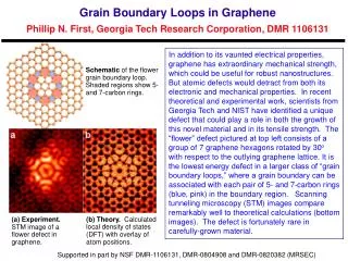
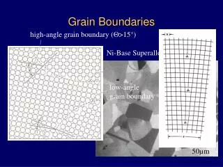
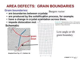
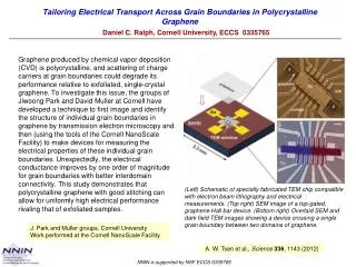
Tailoring Electrical Transport Across Grain Boundaries in Polycrystalline Graphene Daniel C. Ralph, Cornell University, ECCS 0335765 Graphene produced by chemical vapor deposition (CVD) is polycrystalline, and scattering of charge carriers at grain boundaries could degrade its performance relative to exfoliated, single-crystal graphene. To investigate this issue, the groups of Jiwoong Park and David Muller at Cornell have developed a technique to first image and identify the structure of individual grain boundaries in graphene by transmission electron microscopy and then (using the tools of the Cornell NanoScale Facility) to make devices for measuring the electrical properties of these individual grain boundaries. Unexpectedly, the electrical conductance improves by one order of magnitude for grain boundaries with better interdomain connectivity. This study demonstrates that polycrystalline graphene with good stitching can allow for uniformly high electrical performance rivaling that of exfoliated samples. (Left) Schematic of specially fabricated TEM chip compatible with electron beam lithography and electrical measurements. (Top right) SEM image of a top-gated, graphene Hall bar device. (Bottom right) Overlaid SEM and dark field TEM images showing a device crossing a single grain boundary between two domains of graphene. J. Park and Muller groups, Cornell University Work performed at the Cornell NanoScaleFacility A. W. Tsen et al., Science 336, 1143 (2012)