Download
1 / 7
210 likes | 1.35k Views
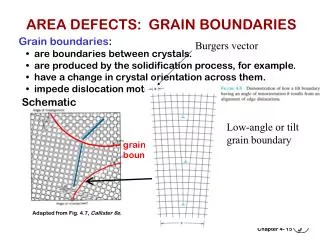
AREA DEFECTS: GRAIN BOUNDARIES. Grain boundaries : • are boundaries between crystals. • are produced by the solidification process, for example. • have a change in crystal orientation across them. • impede dislocation motion. Burgers vector. Schematic.

E N D
AREA DEFECTS: GRAIN BOUNDARIES Grain boundaries: • are boundaries between crystals. • are produced by the solidification process, for example. • have a change in crystal orientation across them. • impede dislocation motion. Burgers vector Schematic Low-angle or tilt grain boundary Adapted from Fig. 4.7, Callister 6e. 15
OTHER DEFECTS: • • External surfaces of a material (where bonds are not complete for atoms). • Stacking faults in FCC materials (i.e. a loss or interruption in the ABCABC… sequence) • Bulk or Volume Defects: like cracks, voids or pores, foreign relatively- large inclusions, other material phases (to be studied more later). • Atomic Vibrations: a function of temperature T (actually define it). Typically 1013 vibrations/second. 15
OPTICAL MICROSCOPY (1) • Useful up to 2000X magnification. • Polishing removes surface features (e.g., scratches) • Etching changes reflectance, depending on crystal orientation. close-packed planes Adapted from Fig. 4.11(b) and (c), Callister 6e. (Fig. 4.11(c) is courtesy of J.E. Burke, General Electric Co. micrograph of Brass (Cu and Zn) 0.75mm 16
OPTICAL MICROSCOPY (2) Grain boundaries... • are imperfections, • are more susceptible to etching, • may be revealed as dark lines, • change direction in a polycrystal. Adapted from Fig. 4.12(a) and (b), Callister 6e. (Fig. 4.12(b) is courtesy of L.C. Smith and C. Brady, the National Bureau of Standards, Washington, DC [now the National Institute of Standards and Technology, Gaithersburg, MD].) Or use line method: measure grain numbers intersecting several (5-10) lines drawn on a photomicrograph. Divide line length by average grain number by magnification. 17
ELECTRON MICROSCOPY • • magnification > 2000X. • • Examples: Transmission Electron Microscope (TEM) Scanning Electron Microscope (SEM) • TEM and SEM use electron beams instead of light beams • SEM pictures a top view of a sample (needs to be electrically conductive but no need for polishing and etching) • TEM “sees” through a thin foil of a specimen. Magnification up to 1,000,000X. Used frequently to study dislocations. • SEM has a great depth of field. Magnification from 10X-50,000X. Real dislocations using TEM 16
SCANNING PROBE MICROSCOPY (SPM) • • resolution in the nanometer range (mags. up to 109X) • • Examples: Scanning Tunneling Microscope (STM), and Atomic Force Microscope (AFM) • SPMs give three-dimensional images with surface topography information. An AFM image of (111) atoms in gold 16
SUMMARY • Point, Line, and Area defects arise in solids. • The number and type of defects can be varied and controlled (e.g., T controls vacancy conc.) • Defects affect material properties (e.g., grain boundaries control crystal slip). • Defects may be desirable or undesirable (e.g., dislocations may be good or bad, depending on whether plastic deformation is desirable or not.) 18