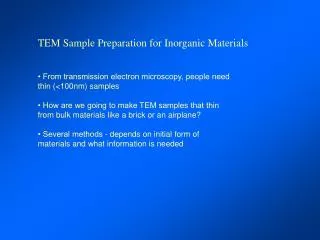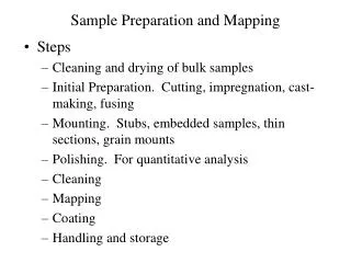
Materials Sample Preparation for TEM
Materials Sample Preparation for TEM. Electron Transparency (thickness < 100 nm) Initial form of the material: particulate or bulk material. Particulate materials (powders, nanoparticles, nanowires).

Materials Sample Preparation for TEM
E N D
Presentation Transcript
Materials Sample Preparation for TEM • Electron Transparency (thickness < 100 nm) • Initial form of the material: particulate or bulk material
Particulate materials (powders, nanoparticles, nanowires) • Desirable particle size is about 500 nm or less. Powders that are more coarse than this should be ground with a mortar and pestle. The specimen preparation consists in transferring a suspension of the particles in a solvent such as isopropanol to a carbon coated grid and letting the solvent evaporate
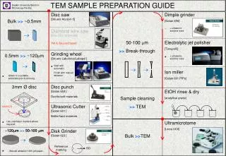
Bulk material • The preparation process can sometimes be time-consuming and often requires careful grinding and polishing techniques, skills for which may take time to develop • All TEM holders accommodate 3-mm disc. Thus, the TEM sample will be in the form of such a disc • Simple metals or single-phase alloys can often be electro polished with an appropriate electrolytic solution. Even multiple phase alloys can sometimes be prepared in this fashion. • More commonly, samples from bulk material are thinned with an ion beam. Before the final ion-beam thinning, however, the sample should be first mechanically thinned by lapping and polishing so that the final thickness in the center of the sample is about 30 microns
Cross section of thin films • Cross-section samples can usually be made using the same ion-thinning process as for bulk samples. However, one must first make a stack by gluing together two or more substrate fragments film-to-film
Particulate material • If particle size is small enough to be electron transparent on its own (<100nm): – Add small amount of powder in solvent – Ultrasonicate to disperse particles well – Place a small drop of suspension on carbon-coated grids – Different types of carbon: amorphous, holey, lacey (increasing pores) • If particle size is larger: – Grind the particle with mortar and pestle – Disperse particles in resin– Microtome using glass or diamond knives (depends on hardness of particles)
Sample Preparation – Bulk Material Procedures: • Initial thinning to make a slice of material between 100-200 mm thick • Cut the 3-mm disk from the bulk • Prethin the central region from one or both faces of the disk to a few micrometers • Final thinning of the disk to electron transparency Note: the method to be used will depend on the information one desired and the physical characteristics of the material (e.g., soft or hard, ductile or brittle…)
Metals dull the diamond Initial thinning • Ductile materials such as metals Example: Chemical wire/string saw A wafering saw (non-diamond) Spark erosion (electro-discharging machining) (is a non-traditional method of removing material by a series of rapidly recurring electric arcing discharges between an electrode (the cutting tool) and the workpiece) Roll the material to thin sheet
Initial thinning • Brittle materials such as ceramics Examples: Si, GaAs, NaCl, MgO can be cleaved with a razor blade Ultramicrotomy, allows for immediate examinantion (diamond wafering saw)
Sheet placed in punch Disc Punch (mechanical) The Disc Punch is ideal for cutting TEM disks from Metals Disk Cutting • Starting materials is ground or sliced (cleaved) to slabs about 200 um in thickness • Then the disc can be cut using ultrasonic disc cutter or the disc punch Ultrasonic Disc Cutter The Ultrasonic Disc Cutter is ideal for cutting TEM disks from brittle materials such as ceramics and semiconductors. Use an abrasive slurry of either boron nitride or silicon carbide
Prethinning the Disk Mechanical Pre-thinning • Disc Grinder: produces high quality parallel-sided thin samples while reducing the chance of sample damage – Grind with SiC sandpaper (60 - 100 - 240 - 400 - 600 grit sizes) – Polish with Al2O3 or diamond suspensions (30 - 15 - 5 - 1 - 0.1μm) Rule of thumb: abrasive produces damage 3x their grit size
Mechanical prethinning: dimpling • The Dimpler provides with the easiest and most reliable means to produce many different types of samples for TEM and can be used on ceramics, many semiconductors, carbons, carbon composites, oxides, borides, silicides, glasses and many others. • When prethinning, the Dimpler produces an ultra-high area for successful, artifact-free ion thinning, while maintaining a greater edge thickness to help prevent breakage while handling. • The thickness achieved will depend on the material being thinned; however, hard specimens typically can be dimpled to less than 5 mm with a 100 mm thick periphery for specimen support.
Dimpling chemically Viewing mirror etchant specimen ‘Jet’ orifice light Example: Dimpling Si using HF + HNO3 GaAs using Br + methanol
How to determine the thickness of Si(110) crystal by transparency colors?
Advantages of the dimpler • Large thin area with thicker rims; • Easier to handle fragile samples; • shorter preparation times; • easier location of the region of interest to be thinned; • large thin area in the center surrounded by thick rim eases handling of the thin samples.
TEM specimen preparation using the Tripod polishers A Tripod Polisher was designed by scientists at IBM, which is used to prepare accurately micro sizes of TEM and SEM samples. For TEM samples, the Tripod Polisher has been used successfully to limit ion milling times to less than 15 minutes, and in some cases, has eliminated the need for ion milling. It can be used to prepare both plan-view and cross-sections from a variety of sample materials, such as ceramics, composites, metals and, geological specimens.
Tripod polishes The point of interest is aligned with the back feet of the Tripod, to ensure the point of interest is coplanar with the back feet. Once the point of the interest has been reached, the polishing plane should be parallel with the back feet.
Tripod polishes General polishing sequence a. 30 um diamond film b. 15 um diamond film c. 3 um diamond film d. 1 um diamond film e. 0.5 um diamond film f. 0.05 um silica Reducing grit size In wedge polishing mode, could generate edge thin enough for TEM
Final thinning Ion Milling – Bombard thin sample with energetic Ar ions, sputter away material until electron transparent – Ar is introduced into an electric field, ionized, accelerated at the sample as a plasma – Variables - ion current, angle of incidence, sample temperature, sample rotation, • High ion current – more damage • Smaller angle of incidence - less implantation, less damage, less preferential sputtering (for composite material or cross sectional interface specimen comprised of with radically dissimilar milling rates For inspection of the specimen
Low Angle Ion Milling (down to 1 degree) Advantages of low angle milling using the single post: 1). Improved surface finish (ion polishing) 2). Larger thin areas while reducing artifacts 3). Less contamination from specimen surroundings 4). Reduced artifacts: (less amorphous layer, less contamination). Milling rates in the PIPS: Below list some typical milling rates at 4º obtained in the PIPS for various materials using one ion gun at 5 keV and no specimen rotation (um/hour for each gun) 1) Copper: 18 2) Silicon: 15 3) Silicon carbide: 8 4) Stainless steel 7 Gatan’s Precision Polishing Ion System (PIPS)
Why rotate the sample? Rotate 360o (at a few rpm) to reduce surface structure (e.g. grooves) generating For cross section TEM specimen, limit the rotation (not 360o) to protect the interface • Why cool the sample? • minimizing atom migration in or on the specimen • limiting phase change at low temperature
Artifact Formation in ion milling Many defects found on Argon ion milled CdTe surface Only growth defects found in iodine-thinned specimen
Final thinning: electropolishing Electropolishing: only be used for electrically conductive samples such as metals and alloys Twin-jet electropolisher
Focused Ion Beam (FIB) milling Similar to SEM? A schematic diagram for the liquid metal ion source FIB system
FIB ions source --- Liquid Metal Ion System (LMIS) 1). heat Ga metal above melting temperature; Ga flows to a W tip with radius ~2-5 um; Others sources: Au, Be, Si, Pd, Ni … 2). use field emission to form 2-5nm Ga tip (“Taylor cone”); 3). extract Ga+ ions and accelerate them down the column 4). Ga flow continuously replenishes source. The principal is a strong electromagnetic field causes the emission of positively charged ions. Why do we need ions instead of electrons: ions are bigger than electrons; they have high interaction probability; since they have high mass, they have slow speed but high momentum and this is good for milling!
d Conventional H-bar technique Find out more on recent advances in FIB from Li, J. et al. Materials Characterization, 57, 64 (2006)
“Lift-out” technique No need for prethinning procedures Risk of losing the sample is also high
In-situ lift-out technique a 200 nm lamella Extraction of the 200 nm lamella using a microgripper inside FIB (Kleindiek nanotechnik) Then transfer onto TEM grid with carbon film