Download
1 / 2
20 likes | 193 Views
Integration of VO 2 with Si (100) Jagdish Narayan, North Carolina State University, DMR 0803663.

E N D
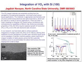
Integration of VO2 with Si (100)Jagdish Narayan, North Carolina State University, DMR 0803663 The VO2 based materials are extremely exciting from the standpoint of fundamental properties and novel smart sensor based applications. The materials in appropriate stoichiometry and structure exhibit sharp electrical and optical transitions, which can be used for a variety of sensor applications. There has been a major challenge to integrate VO2 based sensor architecture with microelectronics capabilities of Silicon chip. Achieving controlled properties of VO2 thin films requires epitaxial growth of monoclinic (P21/c) VO2 on Si (100) with diamond cubic structure. In our research, we have been able to achieve epitaxial integrations of single crystal VO2 films on Si (100) by utilizing yttria-stabilized zirconia (tetragonal) as buffer layer. All these layers grow via the paradigm of domain matching epitaxy, where matching of integral multiples of lattice planes across the film-substrate interface occurs to accommodate the lattice misfit across the scale ranging from small to large. X-ray f scan : demonstration of epitaxial growth of VO2 on Si (100) High resolution TEM micrograph showing atomically sharp interface between VO2 thin film and YSZ intermediate layer. Sharp three orders of magnitude ‘semiconductor to metal transition’ in VO2 films integrated on Si (100)
Integration of VO2 with Si (100) Jagdish Narayan, North Carolina State University, DMR 0803663 The current research impacts profoundly the integration of sensor materials with existing Silicon microelectronics and nanoelectronics technology. This will enable us to create smart sensors and IR camera equipments based upon bolometer imaging arrays that won’t require costly cryogenic cooling. It also has the potential to add multi-functionality to today’s microprocessor chips that are made with Si (100) substrates. NCSU is collaborating with Kopin Corporation on fabrication of next-generation multifunctional smart sensors. This knowledge is also being disseminated to other institutions including minority universities through my Engineering Online course on Materials Science and Processing of Semiconductor Devices. In addition, rising high-school seniors participated in the ASM Materials Camp sponsored by the MSE Department to expose the students to smart materials and sensor applications related to homeland security. Night vision applications High capacity fast responding optical memory devices Smaller, stable, ultrahigh speed sensor devices