Download
1 / 14
140 likes | 235 Views
Semi-Annual Research Review 20-21 July 2000. Consortium for Metrology of Semiconductor Nanodefects. 5 active graduate students, 4 undergrads Michael Jordan and Ping Ding receive Ph.D. DDSURF continued development, Technology Transfer Workshop IV Film capability added to DDSURF

E N D
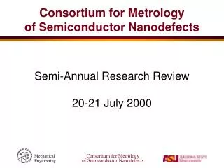
Semi-Annual Research Review 20-21 July 2000 Consortium for Metrologyof Semiconductor Nanodefects
5 active graduate students, 4 undergrads Michael Jordan and Ping Ding receive Ph.D. DDSURF continued development,Technology Transfer Workshop IV Film capability added to DDSURF 5 Technical Papers SRC Project on Hybrid-Emission Defect Instrument Funded ($100k/yr for 3 years) Highlights (1999-2000)
Member Organizations ADE/ADE Optical AMD Applied Materials Duke Scientific Inspex/Hamamatsu KLA-Tencor *cumulative 1996-2000, current members are boldface Lawrence Livermore Labs OSI Inc. Intel SEMATECH Sumitomo Sitix VLSI Standards
Silicon Defects and Optical Wafer Inspection Systems Scatterometer Enhancements Light Scattering by Particles/Defects on CMP Wafers Recently Completed Projects
Process for Fabrication of Standard Pyramidal Pits in Si Artifacts Fabricated, Characterized, and Used in Scattering Experiments Scattering Model Comparison Silicon Defects and Optical Wafer Inspection Systems
In-plane, Differential Scatter of Pyramidal Pits in Si s-polarization incidence angle 65° wavelength 0.6328 µm
In-plane, Differential Scatter of0.34 mm Pyramidal Pit in Si s-polarization incidence angle 65° wavelength 0.6328 µm
New visible wavelength scatterometer designed, built, and tested Provides BRDF measurement capability Competitive specs Used in thesis projects Scatterometer Enhancement
Identified and defined critical CMP defects Acquired standard defect samples Dishing correlation as function of materials Angle-resolved scattering measurements of roughness, patterns, and particles Experimental results in reasonable agreement with models Light Scattering by Particles/Defects on CMP Wafers
Cu SiO2 W SiO2 Dishing: Material and Geometry (Pitch) Dependence Modulus of elasticity: Em(W)=59e-6 lb/in2 Em(Cu)=17e-6 lb/in2 Dishing: at L=10 mm and PD=1/2 D(W)=71.4 nm D(Cu)=144 nm
Natural Scratch and Artifact v-shape, 0.85 mm wide, 95 nm deep scratch on SiO2 - made by diamond tip on AFM v-shape, 1.3 mm wide, 4.7 nm deep scratch on SiO2
Scattering by 0.305 mm PSL Spheres on Si Substrate & on SiO2 Film 0.785-mm SiO2 Si