BASIC COMPUTER ORGANIZATION AND DESIGN
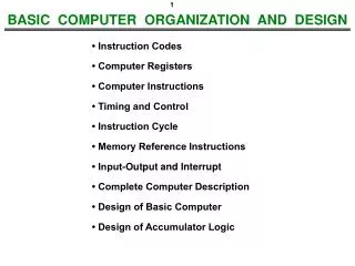
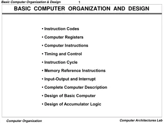
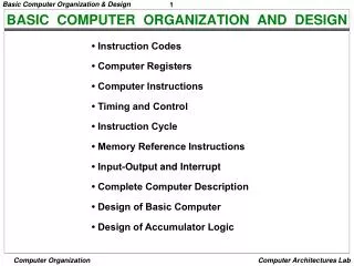
BASIC COMPUTER ORGANIZATION AND DESIGN. • Instruction Codes • Computer Registers • Computer Instructions • Timing and Control • Instruction Cycle • Memory Reference Instructions • Input-Output and Interrupt • Complete Computer Description • Design of Basic Computer

BASIC COMPUTER ORGANIZATION AND DESIGN
E N D
Presentation Transcript
BASIC COMPUTER ORGANIZATION AND DESIGN • Instruction Codes • Computer Registers • Computer Instructions • Timing and Control • Instruction Cycle • Memory Reference Instructions • Input-Output and Interrupt • Complete Computer Description • Design of Basic Computer • Design of Accumulator Logic
Every different processor has its own design (different registers, buses, micro-operations, machine instructions, etc) Modern processor is a very complex device It contains Many registers Multiple arithmetic units, for both integer and floating point calculations The ability to pipeline several consecutive instructions to speed execution Etc. However, to understand how processors work, use a simplified processor model This is similar to what real processors were like ~25 years ago INTRODUCTION
The Basic Computer has two components, a processor and memory The memory has 4096 words in it 4096 = 212, so it takes 12 bits to select a word in memory Each word is 16 bits long THE BASIC COMPUTER RAM CPU 0 15 0 4095
Program A sequence of (machine) instructions (Machine) Instruction A group of bits that tell the computer to perform a specific operation (a sequence of micro-operation) The instructions of a program, along with any needed data are stored in memory The CPU reads the next instruction from memory It is placed in an Instruction Register (IR) Control circuitry in control unit then translates the instruction into the sequence of microoperations necessary to implement it Instruction codes INSTRUCTIONS
A computer instruction is often divided into two parts An opcode (Operation Code) that specifies the operation for that instruction An address that specifies the registers and/or locations in memory to use for that operation In the Basic Computer, since the memory contains 4096 (= 212) words, we needs 12 bit to specify which memory address this instruction will use In the Basic Computer, bit 15 of the instruction specifies the addressing mode (0: direct addressing, 1: indirect addressing) Since the memory words, and hence the instructions, are 16 bits long, that leaves 3 bits for the instruction’s opcode Instruction codes Instruction Format 15 14 12 11 0 Opcode Address I Addressing mode INSTRUCTION FORMAT
The address field of an instruction can represent either Direct address: the address in memory of the data to use (the address of the operand), or Indirect address: the address in memory of the address in memory of the data to use Effective Address (EA) The address, that can be directly used without modification to access an operand for a computation-type instruction, or as the target address for a branch-type instruction Instruction codes Indirect addressing Direct addressing 0 ADD 1 ADD 457 35 300 22 1350 300 Operand 457 1350 Operand + + AC AC ADDRESSING MODES
A processor has many registers to hold instructions, addresses, data, etc The processor has a register, the Program Counter (PC) that holds the memory address of the next instruction Since the memory in the Basic Computer only has 4096 locations, the PC only needs 12 bits In a direct or indirect addressing, the processor needs to keep track of what locations in memory it is addressing: The Address Register (AR) is used for this The AR is a 12 bit register in the Basic Computer When an operand is found, using either direct or indirect addressing, it is placed in the Data Register (DR). The processor then uses this value as data for its operation The Basic Computer has a single general purpose register – the Accumulator (AC) Instruction codes PROCESSOR REGISTERS
The significance of a general purpose register is that it can be used for loading operands and storing results e.g. load AC with the contents of a specific memory location; store the contents of AC into a specified memory location Often a processor will need a scratch register to store intermediate results or other temporary data; in the Basic Computer this is the Temporary Register (TR) The Basic Computer uses a very simple model of input/output (I/O) operations Input devices are considered to send 8 bits of character data to the processor The processor can send 8 bits of character data to output devices The Input Register (INPR) holds an 8 bit character gotten from an input device The Output Register (OUTR) holds an 8 bit character to be send to an output device Instruction codes PROCESSOR REGISTERS
Registers BASIC COMPUTER REGISTERS Registers in the Basic Computer 11 0 PC Memory 11 0 4096 x 16 AR 15 0 IR CPU 15 0 15 0 TR DR 7 0 7 0 15 0 OUTR INPR AC List of Registers • DR 16 Data Register Holds memory operand • AR 12 Address Register Holds address for memory • AC 16 Accumulator Processor register • IR 16 Instruction Register Holds instruction code • PC 12 Program Counter Holds address of instruction • TR 16 Temporary Register Holds temporary data • INPR 8 Input Register Holds input character • OUTR 8 Output Register Holds output character
The registers in the Basic Computer are connected using a bus This gives a savings in circuitry over complete connections between registers Registers COMMON BUS SYSTEM
Registers COMMON BUS SYSTEM S2 S1 Bus S0 Memory unit 7 4096 x 16 Address Write Read AR 1 LD INR CLR PC 2 LD INR CLR DR 3 LD INR CLR E AC 4 ALU LD INR CLR INPR IR 5 LD TR 6 LD INR CLR OUTR Clock LD 16-bit common bus
Registers Read INPR Write Memory 4096 x 16 ALU E Address AC L I C L I C L DR IR L I C L I C TR PC OUTR L AR L I C 7 1 2 3 4 5 6 16-bit Common Bus COMMON BUS SYSTEM S0 S1 S2
Three control lines, S2, S1, and S0 control which register the bus selects as its input Either one of the registers will have its load signal activated, or the memory will have its read signal activated Will determine where the data from the bus gets loaded The 12-bit registers, AR and PC, have 0’s loaded onto the bus in the high order 4 bit positions When the 8-bit register OUTR is loaded from the bus, the data comes from the low order 8 bits on the bus Registers COMMON BUS SYSTEM S2 S1 S0 Register 0 0 0 x 0 0 1 AR 0 1 0 PC 0 1 1 DR 1 0 0 AC 1 0 1 IR 1 1 0 TR 1 1 1 Memory
Instructions 15 12 11 0 Register operation 0 1 1 1 15 12 11 0 I/O operation 1 1 1 1 BASIC COMPUTER INSTRUCTIONS • Basic Computer Instruction Format Memory-Reference Instructions (OP-code = 000 ~ 110) 15 14 12 11 0 Opcode Address I Register-Reference Instructions (OP-code = 111, I = 0) Input-Output Instructions (OP-code =111, I = 1)
Instructions BASIC COMPUTER INSTRUCTIONS Hex Code Symbol I = 0 I = 1 Description • AND 0xxx 8xxx AND memory word to AC • ADD 1xxx 9xxx Add memory word to AC • LDA 2xxx Axxx Load AC from memory • STA 3xxx Bxxx Store content of AC into memory • BUN 4xxx Cxxx Branch unconditionally • BSA 5xxx Dxxx Branch and save return address • ISZ 6xxx Exxx Increment and skip if zero • CLA 7800 Clear AC • CLE 7400 Clear E • CMA 7200 Complement AC • CME 7100 Complement E • CIR 7080 Circulate right AC and E • CIL 7040 Circulate left AC and E • INC 7020 Increment AC • SPA 7010 Skip next instr. if AC is positive • SNA 7008 Skip next instr. if AC is negative • SZA 7004 Skip next instr. if AC is zero • SZE 7002 Skip next instr. if E is zero • HLT 7001 Halt computer • INP F800 Input character to AC • OUT F400 Output character from AC • SKI F200 Skip on input flag • SKO F100 Skip on output flag • ION F080 Interrupt on • IOF F040 Interrupt off
Instructions INSTRUCTION SET COMPLETENESS Set of instructions using which user can construct machine language programs to evaluate any computable function. • Instruction Types • Functional Instructions • - Arithmetic, logic, and shift instructions • - ADD, CMA, INC, CIR, CIL, AND, CLA (other than ADD/AND?) • Transfer Instructions • - Data transfers between the main memory • and the processor registers • - LDA, STA • Control Instructions • - Program sequencing and control • - BUN, BSA, ISZ • Input/Output Instructions • - Input and output • - INP, OUT
Control unit (CU) of a processor translates from machine instructions to the control signals (for the microoperations) that implement them Control units are implemented in one of two ways Hardwired Control CU is made up of sequential and combinational circuits to generate the control signals Microprogrammed Control A control memory on the processor contains microprograms that activate the necessary control signals We will consider a hardwired implementation of the control unit for the Basic Computer Instruction codes CONTROL UNIT
Timing and control TIMING AND CONTROL Control unit of Basic Computer Instruction register (IR) 14 13 12 15 11 - 0 Other inputs 3 x 8 decoder 7 6 5 4 3 2 1 0 D 0 Combinational Control logic I D Control signals 7 T 15 T 0 15 14 . . . . 2 1 0 4 x 16 decoder Increment (INR) 4-bit sequence Clear (CLR) counter Clock (SC)
Timing and control TIMING SIGNALS - Generated by 4-bit sequence counter and 416 decoder - The SC can be incremented or cleared. - Example: T0, T1, T2, T3, T4, T0, T1, . . . Assume: At time T4, SC is cleared to 0 if decoder output D3 is active. D3T4: SC 0
In Basic Computer, a machine instruction is executed in the following cycle: Fetch an instruction from memory Decode the instruction and calculate effective address (EA) Read the EA from memory if the instruction has an indirect address (Fetch operand) Execute the instruction After an instruction is executed, the cycle starts again at step 1, for the next instruction Note: Every different processor has its own (different) instruction cycle INSTRUCTION CYCLE
Instruction Cycle FETCH and DECODE • Fetch and Decode T0: AR PC (S0S1S2=010, T0=1) T1: IR M [AR], PC PC + 1 (S0S1S2=111, T1=1) T2: D0, . . . , D7 Decode IR(12-14), AR IR(0-11), I IR(15) T1 S2 Bus T0 S1 S0 Memory 7 unit Address Read AR 1 LD PC 2 INR IR 5 LD Clock Common bus
Instrction Cycle DETERMINE THE TYPE OF INSTRUCTION Start SC 0 T0 AR PC T1 IR M[AR], PC PC + 1 T2 Decode Opcode in IR(12-14), AR IR(0-11), I IR(15) (Register or I/O) = 1 = 0 (Memory-reference) =>opcode ≠ 111 D7 = 0 (direct) (I/O) = 1 = 0 (register) (indirect) = 1 I I T3 T3 T3 T3 Nothing Execute Execute AR M[AR] input-output register-reference instruction instruction SC 0 SC 0 Execute T4 memory-reference instruction SC 0 D'7IT3: AR M[AR] D'7I'T3: Nothing D7I'T3: Execute a register-reference instr. D7IT3: Execute an input-output instr.
Instruction Cycle REGISTER REFERENCE INSTRUCTIONS Register Reference Instructions are identified when - D7 = 1, I = 0 - Register Ref. Instr. is specified in b0 ~ b11 of IR - Execution starts with timing signal T3 r = D7 IT3 => Register Reference Instruction Bi = IR(i) , i=0,1,2,...,11 r: SC 0 CLA rB11: AC 0 CLE rB10: E 0 CMA rB9: AC AC’ CME rB8: E E’ CIR rB7: AC shr AC, AC(15) E, E AC(0) CIL rB6: AC shl AC, AC(0) E, E AC(15) INC rB5: AC AC + 1 SPA rB4: if (AC(15) = 0) then (PC PC+1) SNA rB3: if (AC(15) = 1) then (PC PC+1) SZA rB2: if (AC = 0) then (PC PC+1) SZE rB1: if (E = 0) then (PC PC+1) HLT rB0: S 0 (S is a start-stop flip-flop)
MR Instructions MEMORY REFERENCE INSTRUCTIONS Operation Decoder Symbol Symbolic Description AND D0 AC AC M[AR] ADD D1 AC AC + M[AR], E Cout LDA D2 AC M[AR] STA D3 M[AR] AC BUN D4 PC AR BSA D5 M[AR] PC, PC AR + 1 ISZ D6M[AR] M[AR] + 1, if M[AR] + 1 = 0 then PC PC+1 - The effective address of the instruction is in AR and was placed there during timing signal T2 when I = 0, or during timing signal T3 when I = 1 - Memory cycle is assumed to be short enough to complete in a CPU cycle - The execution of MR instruction starts with T4 AND to AC D0T4: DR M[AR] Read operand D0T5: AC AC DR, SC 0 AND with AC ADD to AC D1T4: DR M[AR] Read operand D1T5: AC AC + DR, E Cout, SC 0 Add to AC and store carry in E
MEMORY REFERENCE INSTRUCTIONS LDA: Load to AC D2T4: DR M[AR] D2T5: AC DR, SC 0 STA: Store AC D3T4: M[AR] AC, SC 0 BUN: Branch Unconditionally D4T4: PC AR, SC 0 BSA: Branch and Save Return Address Memory, PC, AR at time T4 Memory, PC after execution 20 0 BSA 135 20 0 BSA 135 PC = 21 Next instruction 21 Next instruction AR = 135 135 21 136 Subroutine Subroutine PC = 136 1 BUN 135 1 BUN 135 Memory Memory
MR Instructions MEMORY REFERENCE INSTRUCTIONS BSA: D5T4: M[AR] PC, AR AR + 1 D5T5: PC AR, SC 0 ISZ: Increment and Skip-if-Zero D6T4: DR M[AR] D6T5: DR DR + 1 D6T4: M[AR] DR, if (DR = 0) then (PC PC + 1), SC 0
MR Instructions FLOWCHART FOR MEMORY REFERENCE INSTRUCTIONS Memory-reference instruction AND ADD LDA STA D T D T D T D T 4 1 4 2 4 3 4 0 M[AR] AC DR M[AR] DR M[AR] DR M[AR] SC 0 D T D T D T 0 5 1 5 2 5 AC AC DR AC DR AC AC + DR SC 0 SC 0 E Cout SC 0 BUN BSA ISZ D T D T D T 4 4 5 4 6 4 PC AR M[AR] PC DR M[AR] SC 0 AR AR + 1 D T D T 5 5 6 5 DR DR + 1 PC AR SC 0 D T 6 6 M[AR] DR If (DR = 0) then (PC PC + 1) SC 0
I/O and Interrupt INPUT-OUTPUT AND INTERRUPT A Terminal with a keyboard and a Printer • Input-Output Configuration Serial Computer registers and flip-flops Input-output communication terminal interface Receiver Printer OUTR FGO interface AC Transmitter Keyboard INPR FGI interface INPR Input register - 8 bits OUTR Output register - 8 bits FGI Input flag - 1 bit FGO Output flag - 1 bit IEN Interrupt enable - 1 bit Serial Communications Path Parallel Communications Path - The terminal sends and receives serial information - The serial info. from the keyboard is shifted into INPR - The serial info. for the printer is stored in the OUTR - INPR and OUTR communicate with the terminal serially and with the AC in parallel. - The flags are needed to synchronize the timing difference between I/O device and the computer
I/O and Interrupt PROGRAM CONTROLLED DATA TRANSFER -- CPU -- -- I/O Device -- loop: If FGI = 0 goto loop AC INPR, FGI 0 /* Output */ /* Initially FGO = 1 */ loop: If FGO = 0 goto loop OUTR AC, FGO 0 /* Input */ /* Initially FGI = 0 */ loop: If FGI = 1goto loop INPR new data, FGI 1 loop: If FGO = 1goto loop consume OUTR, FGO 1 FGI=0 FGO=1 Start Input Start Output yes yes FGI=0 FGO=1 no no AC INPR consume OUTR FGO 1 yes More Character More Character yes no END no END
INPUT-OUTPUT INSTRUCTIONS CPU Side D7IT3 = p IR(i) = Bi, i = 6, …, 11 p: SC 0 Clear SC INP pB11: AC(0-7) INPR, FGI 0 Input char. to AC OUT pB10: OUTR AC(0-7), FGO 0 Output char. from AC SKI pB9: if(FGI = 1) then (PC PC + 1) Skip on input flag SKO pB8: if(FGO = 1) then (PC PC + 1) Skip on output flag ION pB7: IEN 1 Interrupt enable on IOF pB6: IEN 0 Interrupt enable off
I/O and Interrupt PROGRAM-CONTROLLED INPUT/OUTPUT • Program-controlled I/O - Continuous CPU involvement I/O takes valuable CPU time - CPU slowed down to I/O speed - Simple - Least hardware Input LOOPSKI DEV BUN LOOP INP DEV Output LDA DATA LOOP SKO DEV BUN LOOP OUT DEV
INTERRUPT INITIATED INPUT/OUTPUT - Open communication only when some data has to be passed --> interrupt. - The I/O interface, instead of the CPU, monitors the I/O device. - When the interface founds that the I/O device is ready for data transfer, it generates an interrupt request to the CPU - Upon detecting an interrupt, the CPU stops momentarily the task it is doing, branches to the service routine to process the data transfer, and then returns to the task it was performing. * IEN (Interrupt-enable flip-flop) - can be set and cleared by instructions - when cleared, the computer cannot be interrupted
I/O and Interrupt FLOWCHART FOR INTERRUPT CYCLE R = Interrupt f/f =0 Instruction cycle =1 Interrupt cycle R Store return address Fetch and decode in location 0 instructions M[0] PC =0 Execute IEN instructions =1 Branch to location 1 PC 1 =1 FGI =0 IEN 0 R 0 =1 FGO =0 R 1 - The interrupt cycle is a HW implementation of a branch and save return address operation. - At the beginning of the next instruction cycle, the instruction that is read from memory is in address 1. - At memory address 1, the programmer must store a branch instruction that sends the control to an interrupt service routine - The instruction that returns the control to the original program is "indirect BUN 0"
I/O and Interrupt REGISTER TRANSFER OPERATIONS IN INTERRUPT CYCLE Memory Before interrupt After interrupt cycle 256 0 0 1 0 BUN 1120 PC = 1 0 BUN 1120 Main Main 255 255 Program Program PC = 256 256 1120 1120 I/O I/O Program Program 1 BUN 0 1 BUN 0 Register Transfer Statements for Interrupt Cycle - R F/F 1 if IEN (FGI + FGO)T0T1T2 T0T1T2 (IEN)(FGI + FGO): R 1 - The fetch and decode phases of the instruction cycle must be modified Replace T0, T1, T2 with R'T0, R'T1, R'T2 - The interrupt cycle : RT0: AR 0, TR PC RT1: M[AR] TR, PC 0 RT2: PC PC + 1, IEN 0, R 0, SC 0
I/O and Interrupt FURTHER QUESTIONS ON INTERRUPT • How can the CPU recognize the device • requesting an interrupt ? • Since different devices are likely to require • different interrupt service routines, how can • the CPU obtain the starting address of the • appropriate routine in each case ? • Should any device be allowed to interrupt the • CPU while another interrupt is being serviced ? • How can the situation be handled when two or • more interrupt requests occur simultaneously ?
Description COMPLETE COMPUTER DESCRIPTIONFlowchart of Operations start SC 0 =0(Instruction =1 (interrupt Cycle) Cycle) R RT0 R’T0 AR 0, TR PC AR PC R’T1 RT1 IR M[AR], PC PC + 1 M[AR] TR, PC 0 R’T2 RT2 AR IR(0~11), I IR(15) D0...D7 Decode IR(12 ~ 14) PC PC + 1, IEN 0 R 0, SC 0 =1(Register or I/O) =0(Memory Ref) D7 =1 (I/O) =0 (Register) =1(Indir) =0(Dir) I I =0 IEN =1 D7IT3 D7I’T3 D7’IT3 D7’I’T3 =1 AR <- M[AR] Execute RR Instruction Idle Execute I/O Instruction FGI =0 =1 D7’T4 FGO Execute MR Instruction =0 R 1
Description COMPLETE COMPUTER DESCRIPTION Microoperations Fetch Decode Indirect Interrupt Memory-Reference AND ADD LDA STA BUN BSA ISZ RT0: RT1: RT2: D7IT3: RT0: RT1: RT2: D0T4: D0T5: D1T4: D1T5: D2T4: D2T5: D3T4: D4T4: D5T4: D5T5: D6T4: D6T5: D6T6: AR PC IR M[AR], PC PC + 1 D0, ..., D7 Decode IR(12 ~ 14), AR IR(0 ~ 11), I IR(15) AR M[AR] R 1 AR 0, TR PC M[AR] TR, PC 0 PC PC + 1, IEN 0, R 0, SC 0 DR M[AR] AC AC DR, SC 0 DR M[AR] AC AC + DR, E Cout, SC 0 DR M[AR] AC DR, SC 0 M[AR] AC, SC 0 PC AR, SC 0 M[AR] PC, AR AR + 1 PC AR, SC 0 DR M[AR] DR DR + 1 M[AR] DR, if(DR=0) then (PC PC + 1), SC 0 T0T1T2(IEN)(FGI + FGO):
Description COMPLETE COMPUTER DESCRIPTION Microoperations Register-Reference CLA CLE CMA CME CIR CIL INC SPA SNA SZA SZE HLT Input-Output INP OUT SKI SKO ION IOF D7IT3 = r IR(i) = Bi r: rB11: rB10: rB9: rB8: rB7: rB6: rB5: rB4: rB3: rB2: rB1: rB0: D7IT3 = p IR(i) = Bi p: pB11: pB10: pB9: pB8: pB7: pB6: (Common to all register-reference instr) (i = 0,1,2, ..., 11) SC 0 AC 0 E 0 AC AC E E AC shr AC, AC(15) E, E AC(0) AC shl AC, AC(0) E, E AC(15) AC AC + 1 If(AC(15) =0) then (PC PC + 1) If(AC(15) =1) then (PC PC + 1) If(AC = 0) then (PC PC + 1) If(E=0) then (PC PC + 1) S 0 (Common to all input-output instructions) (i = 6,7,8,9,10,11) SC 0 AC(0-7) INPR, FGI 0 OUTR AC(0-7), FGO 0 If(FGI=1) then (PC PC + 1) If(FGO=1) then (PC PC + 1) IEN 1 IEN 0
Design of Basic Computer DESIGN OF BASIC COMPUTER(BC) Hardware Components of BC A memory unit: 4096 x 16. Registers: AR, PC, DR, AC, IR, TR, OUTR, INPR, and SC Flip-Flops(Status): I, S, E, R, IEN, FGI, and FGO Decoders: a 3x8 Opcode decoder a 4x16 timing decoder Common bus: 16 bits Control logic gates: Adder and Logic circuit: Connected to AC Control Logic Gates • - Input Controls of the nine registers • - Read and Write Controls of memory • - Set, Clear, or Complement Controls of the flip-flops • - S2, S1, S0 Controls to select a register for the bus • - AC, and Adder and Logic circuit
Design of Basic Computer 12 12 From bus To bus AR D' 7 I Clock LD T 3 T INR 2 CLR R T 0 D T 4 CONTROL OF REGISTERS AND MEMORY Address Register; AR Scan all of the register transfer statements that change the content of AR: R’T0: AR PC LD(AR) R’T2: AR IR(0-11) LD(AR) D’7IT3: AR M[AR] LD(AR) RT0: AR 0 CLR(AR) D5T4: AR AR + 1 INR(AR) LD(AR) = R'T0 + R'T2 + D'7IT3 CLR(AR) = RT0 INR(AR) = D5T4
Design of Basic Computer D 7 p I J IEN Q B 7 T3 B 6 K R T 2 CONTROL OF FLAGS IEN: Interrupt Enable Flag pB7: IEN 1 (I/O Instruction) pB6: IEN 0 (I/O Instruction) RT2: IEN 0 (Interrupt) p = D7IT3 (Input/Output Instruction)
Design of Basic Computer x1 S x2 2 Multiplexer x3 Encoder bus select S x4 1 x5 inputs S x6 0 x7 CONTROL OF COMMON BUS selected register x1 x2 x3 x4 x5 x6 x7 S2 S1 S0 0 0 0 0 0 0 0 0 0 0 none 1 0 0 0 0 0 0 0 0 1 AR 0 1 0 0 0 0 0 0 1 0 PC 0 0 1 0 0 0 0 0 1 1 DR 0 0 0 1 0 0 0 1 0 0 AC 0 0 0 0 1 0 0 1 0 1 IR 0 0 0 0 0 1 0 1 1 0 TR 0 0 0 0 0 0 1 1 1 1 Memory x1 for placing AR onto bus D4T4: PC AR D5T5: PC AR x1 = D4T4 + D5T5
Design of AC Logic 16 Adder and 16 16 16 AC logic From DR circuit To bus 8 From INPR LD INR CLR Clock Control gates DESIGN OF ACCUMULATOR LOGIC Circuits associated with AC All the statements that change the content of AC D0T5: AC AC DR AND with DR D1T5: AC AC + DR Add with DR D2T5: AC DR Transfer from DR pB11: AC(0-7) INPR Transfer from INPR rB9: AC AC Complement rB7 : AC shr AC, AC(15) E Shift right rB6 : AC shl AC, AC(0) E Shift left rB11 : AC 0 Clear rB5 : AC AC + 1 Increment
Design of AC Logic 16 16 From Adder To bus AC and Logic D AND Clock 0 LD T 5 INR D ADD 1 CLR D DR 2 T 5 p INPR B 11 r COM B 9 SHR B 7 SHL B 6 INC B 5 CLR B 11 CONTROL OF AC REGISTER Gate structures for controlling the LD, INR, and CLR of AC
Design of AC Logic ALU (Adder & Logic Circuits)