Download
1 / 1
20 likes | 164 Views
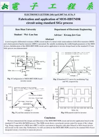
ELECTRONICS LETTERS 26th April 2007 Vol. 43 No. 9. Fabrication and application of MOS-HBTNDR circuit using standard SiGe process. Kun Shan University. Department of Electronic Engineering. Student : Wei -Lun Sun. Advisor : Kwang-Jow Gan. Abstract

E N D
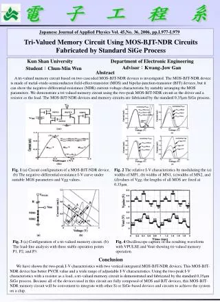
ELECTRONICS LETTERS 26th April 2007 Vol. 43 No. 9 Fabrication and application of MOS-HBTNDR circuit using standard SiGe process Kun Shan University Department of Electronic Engineering Student:Wei -Lun Sun Advisor:Kwang-Jow Gan Abstract A novel negative differential resistance (NDR) circuit made of a metal-oxide-semiconductor field-effect-transistor (MOS) and a heterojunction bipolar transistor (HBT) is presented. By suitably modulating the width=length parameters of the MOS devices, thefabrication of this MOS-HBT-NDR circuit and its application to inverter design based on the standard 0.35 mm SiGe process was demonstrated. Fig. 1 Configuration of MOS-HBT-NDR-based inverter circuit Fig. 2 Simulated I-V curves by modulating Vgg and VG, respectively Fig. 3 Load-line analysis for inverter Fig. 4 Measured result for inverter Conclusion We have demonstrated the design and fabrication of the MOS-HBT-NDR circuit and inverter application based on the standard 0.35 mm SiGe BiCMOS process. This NDR circuit shows a good peak current control by means of the voltage Vgg. Being composed of a MOS and a HBT, it will be convenient to integrate with other Sibased or SiGe-based devices and circuits on the same chip. Furthermore, we still can fabricate this MOS-HBT-NDR circuit by the standard SiGe-based integrated circuit, even down to nanoscale process.