Download
1 / 21
1.03k likes | 3.76k Views
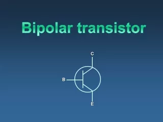
Standard Bipolar Transistor Fabrication Process. In this lecture, you will learn the integration of the processes in the fabrication of a standard buried collector bipolar transistor. Read : 1. C.Y. Chang and S.M. Sze, “ULSI Technology”, McGraw-Hill, (1996), pp. 495-497.

E N D
In this lecture, you will learn • the integration of the processes in the fabrication of a standard buried collector bipolar transistor. • Read : • 1. C.Y. Chang and S.M. Sze, “ULSI Technology”, McGraw-Hill, (1996), pp. 495-497. • 2. R.C. Jaeger, “Modular Series on Solid State Devices, Vol V : Introduction to Microelectronic Fabrication”, Prentice-Hall, (2002), pp. 10-12, 233-243.
The basic junction-isolated bipolar transistor fabrication process is known as the standard buried collector (SBC) process. • The SBC process is the primary process used in the fabrication of analog and power bipolar ICs with power supplies exceeding about 15V. • For digital ICs, the SBC process has been replaced by other fabrication processes using other isolation techniques.
1. Oxide growth A lightly doped p-type silicon wafer is used as the substrate, for the fabrication of an n-p-n bipolar transistor. On this wafer, a silicon dioxide layer is grown by heating the wafer in oxygen or steam in a furnace. This oxide layer will acts as the mask for the next step of the fabrication process.
2. Buried layer formation A window is opened in the oxide layer by photolithography. Antimony ions are implanted into the substrate to form a heavily doped n-type buried layer, also known as the sub-collector. The function of this buried layer is to reduce the resistance of the collector of the bipolar transistor. The masking oxide layer is then removed by wet etching. Q. Why is antimony used as the dopant ?
3. Epitaxial growth An n-type epitaxial layer is grown on top of the silicon wafer. The epitaxial growth process results in a high-quality silicon layer with the same crystal structure as the original silicon wafer. The doping is chosen so as to give the desired collector-base junction breakdown voltage. The thickness is chosen so that the collector-base junction space-charge region (SCR) just extends across the entire epitaxial layer when the maximum collector-base junction reverse bias voltage is applied.
4. Device Isolation A masking oxide is grown. Windows are etched in the oxide using photolithography. Boron ions are implanted into the exposed part of the underlying epitaxial layer to form heavily doped p-type regions. The boron ions are driven through the epitaxial layer by thermal diffusion, until they reach the substrate. Islands in the epitaxial layer will be formed, thus effectively isolating the transistors, which are to be built in the epitaxial layer, from one another.
5. Base formation A thermal oxide is grown and a window opened in the oxide by photolithography. Boron ions are implanted into the exposed part of the epitaxial layer with a sufficient dose to convert it into a p-type region. The boron ions are diffused further into the epitaxial layer to form the base of the transistor.
6. Emitter formation A thermal oxide is grown and windows are opened in the oxide by photolithography. A heavy dose of phosphorus is implanted into the exposed areas. The phosphorus ions convert the part of the base into which it is implanted into an n+ regions, forming the emitter. An n+ region is also formed in the exposed part of the n-type collector region, in order to facilitate the formation of a good ohmic contact.
7. Contact window opening A thermal oxide is grown. Using photolithography, windows are etched in the oxide to expose parts of the emitter, base and collector regions. This is to allow metal contacts to be made to these regions.
8. Metal contact formation Aluminium is evaporated onto the wafer by vacuum evaporation. The excess aluminium are etched away, using photolithography, leaving only those that are needed to make contact with the emitter, base and collector of the transistor. In an integrated circuit, metal tracks may be defined to interconnect the various parts of the transistor to other circuit elements.
Question : A major disadvantage of the SBC process described above is the large area occupied by the entire transistor structure relative to the active area of the transistor, which is the area directly below the emitter. Which process takes up the most space, and what can be done to reduce this area ?
Link to the Flash animation on the fabrication of the standard buried collector bipolar transistor : BJT Fabrication