Download
1 / 9
90 likes | 266 Views
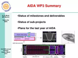
AIDA WP3 Annual Meeting. Status of milestones and deliverables P2 Report Plans for last year of AIDA Agenda. Objectives. Sub Projects. WP3.2 (3D interconnection)

E N D
AIDA WP3 Annual Meeting • Status of milestones and deliverables • P2 Report • Plans for last year of AIDA • Agenda
Sub Projects • WP3.2 (3D interconnection) • Bonn/CPPM: Interconnection of the ATLAS FEI4 chips to sensors using bump bonding and TSVs from IZM (large diameter TSV, large interconnection pitch). • CERN: Interconnection of MEDIPIX3 chips using the CEA-LETI process • INFN/IPHC-IRFU: Interconnection of chips from Tezzaron/Chartered to edgeless sensors and/or CMOS sensors using an advanced interconnection process (T-MICRO or others) • LAL/LAPP/LPNHE/MPP: Readout ASICs in 65nm technology interconnected to pixel sensors using the CEA-LETI or EMFT process. • MPP/GLA/LAL/LIV/LPNHE:Interconnection of ATLAS FEI4 chips to sensors using SLID interconnection and ICV (high density TSVs) from EMFT. • UB: 3D interconnection of 2 layers of Geiger-Mode APD arrays with integrated readout in Tezzaron Chartered technology. • RAL/UPPSALAIntegrationof a 2-Tier readout ASIC for a CZT pixel sensor using EMFT SLID technology and TSV including redistribution of I/O connections to the backside for a 4-side buttable device. • WP3.3 (IP blocks) • IP blocks in 65 nm CMOS (coordinated by CERN): The choice of the 65 nm CMOS generation wasprompted by the needs of future vertex detectors, which can benefit from modernnanoscaletechnologies by obtainingsmaller and more intelligentpixels in pixel detectors, more compact digitallogic and lowerpower in front-end chips. • IP blocks in SiGe (coordinated by LAL-CNRS): provide IP blocks for needs in calorimeters and TPCs. These two domains are demanding in high dynamic range and precision, so the choice of technology would be to use Silicon Germanium (SiGe).
Milestones post-poned Milestone achieved if some of the subprojects are successful
Deliverables postponed Deliverable achieved if some of the subprojects are successful
P2 Report Report due now Draft exists (see AIDA WWW pages) Need to update and finalize report based on this meeting’s reports Also, need to update status of old milestones and deliverables: e.g.D2.5 (Wafer post-processing – thinning, TSV (was due M25)
Next year’s objectives • WP3.2 • Deliverable D3.8: detectors available for 3D assessment • -> already achieved by CERN • Deliverable D3.10:Assemsent of 3D integrated sensors • -> push all subprojects to achieve deliverables • (discuss: projects relying on 65nm and Tezzaron) • Assess performance of 3D sensors but also: • cost, processing time • technological challenges • experience with industry and vendors • recommendation for further R&D • WP3.3 • Deliverables D3.4 (postponed) and D3.9 • Need discussion how to proceed with 65nm