Download
1 / 1
10 likes | 156 Views
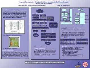
ID Stage. logic. EX Stage. Instruction FF. DNCloopFF. DMT Decode. Instruction decode. hhhh decode (DMT type). decode. Multi_cycle FF. dma_cycle. signals. data/base reg index. memRD_en. Skip_inc FF. memWR_en. datapath. datapath. mem_addr. latchDBR_FF. DMA signals. ubyteload.

E N D
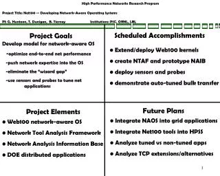
ID Stage logic EX Stage Instruction FF DNCloopFF DMT Decode Instruction decode hhhh decode (DMT type) decode Multi_cycle FF dma_cycle signals data/base reg index memRD_en Skip_inc FF memWR_en datapath datapath mem_addr latchDBR_FF DMA signals ubyteload latch OffsetFF MMU Address/data Registers DMAfsm DMT type hhhh Design and Implementation of Multiple-Load/Store Instruction Set for Wireless Integrated Microsystems Microcontroller Students: Amlan Ghosh, Jeff Campbell, Nathaniel Gaskin, Spencer Kellis Faculty: Prof. Richard B. Brown Project Goals A Multiple Ld/St instruction set (named as DMA) has been integrated with the WIMS microcontroller to enhance data transfer between memory and the loop cache by providing dedicated instructions to fill the loop cache quickly without incurring the overhead of numerous load-store instructions. These instructions will allow a compiler-managed dynamic loop-cache filling algorithm to control fast, low-power transfers of an entire register window occuring upon branches to or from subroutines and interrupt handlers. Overall power requirements can thereby be reduced, further enhancing the performance and utility of the microcontroller. Architectural Specification Instruction level model (C Simulator) Digital model (Verilog) • Single Instruction Verification • Random Code generator based instruction • Application code based • verification Assembler & Compiler Behavioral Verification (Verilog Simulator) Cross-domain Verification (Instruction level model compared with digital model) Application code development Application code development Synthesis/PR/Timing (Synthesis Tool) Analog Macro Mechanical Macro (a) (b) Back Annotated Compiler & Instruction-Level Model Extraction, Timing (Timing Tool) Fig. 4 (a) Block Diagram of Multiple-Ld/St Instryction set hardware implemntation Fig. 4 (b) Finite state machine of decode stage for Multiple-Ld/St instructions Cross-domain Verification (Annotated Instruction level model compared with digital model) Results The NanoSim power analysis shows conclusive power (Table 1) and execution time (Table 2) savings in the pipeline block of the WIMS MCU between DMA and non-DMA implementation of memory accesses. Although DMA instructions certainly will not account for the main body of code, their efficiency could account for relatively large power savings across the entire chip. Application Code Digital Macro Macro Place Route, Layout Verification: DRC & LVS (APR & IC Tools) Code Release Fig 1: Block Diagram of Microcontroller Architecture Layout Parasitic Extraction and Back Annotation (IC Tools) Table 1 Table 2 Cross Domain Verification (Verilog with updated Verilog-A with interconnect parasitics) Tapeout Fig 4: Top-down Design Methodology • Future work • Inclusion of low power library cells for specific power-hungry blocks and customized circuits with low-power topologies • Reducing power dissipation by Dynamic Voltage and Frequency Scaling • Adding standby/sleep mode during no-operation of hardware/memory using clock and power gating • Integration with analog/RF frontend • Using multiple banked memory which will allow some banks to be turned off - reducing address line capacitance Fig 2: Layout of WIMS Microcontroller Design and Implementation In a DMA load/store operation the source and destination registers can be any of the address registers, data registers, memory-mapped registers or loop cache locations. All possible operations of the data transfer depend upon the offset register and Direct Memory Type (DMT) specification. This eliminates calls to memory in the fetch stage for subsequent instructions while the DMA instruction is executing. Approach and Methodology The DMA implementation has been incorporated using Verilog-XL, maintaining an inclination towards semi-structural code in order to customize design for low power and decreased area. The architecture has been verified using a combination of C simulators and Matlab code. Different levels of verification (single instruction based, random code generation based, and application code based) has been employed for an exhaustive test of the functionality of the codes to ensure proper behavior of the circuitry. Acknowledgements: Eric D. Marsman & Robert M. Senger, University of Michigan, Ann Arbor