Digital Audio Controller 2302
Digital Audio Controller 2302. Ece345 Senior Design Project by Todd “Slave-Driver” Konecny Jay “Late-Night” Burgett Insoo “Ninja” Shin April 25, 2001. Introduction.

Digital Audio Controller 2302
E N D
Presentation Transcript
Digital Audio Controller 2302 Ece345 Senior Design Project by Todd “Slave-Driver” Konecny Jay “Late-Night” Burgett Insoo “Ninja” Shin April 25, 2001
Introduction Based on an overall team interest in DSP coding and a desire to experiment with analog circuitry, we proposed to create the Digital Audio Controller 2302. This project was intended to emphasize an exploration in operational amplifier theory and the use of digital filtering to create a high-fidelity device that could be used in the real world.
Project Objective • To design a high fidelity audio spectrum controller using digital and analog components that is compatible with professional audio equipment.
Device Description • Audio crossover to be accessed by D.J.’s to control a sound system’s response, much like a conventional equalizer, but with limited, more powerful controls. • Hybrid design using digital filters and analog amplifiers to modify a stereo program by altering band gains and/or selectively muting bands.
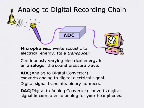
Device Description • Accepts a stereo analog program as input. • DSP divides the stereo program into six bands: right and left lows, mids, and highs. • Analog circuitry accepts these six signals and controls stereo pairs of bands with three potentiometers and three mute buttons. • Analog circuitry recombines the bands and outputs a stereo program.
Software Overview • High and low-pass filters designed using Matlab. • FIR filters guarantee linear phase shift across the spectrum. • High number of coefficients provides for < 1% magnitude ripple. • View response using Matlab’s graphing functions.
Software Overview • Initial filter. • Removes aliasing error caused by filters on DSP board allowing frequencies greater than the Nyquist frequency into A/D converters. • Low-pass at 18khz.
Software Overview Initial Filter Response
Software Overview • Second filter (diagram). • High-pass filter at 3kHz produces high band. • Delay included to re-align high bands with mid and low bands after multi-rate occurs. • Third filter (diagram). • Low-pass filter at 3kHz. • Output contains mid and low bands information.
Software Overview Second and Third Filter Response
Software Overview • Down-sample by 3. • Allows for smoother low and mid-pass filter responses. • Consists of making every second and third sample equal to zero.
Software Overview • Fourth filter (diagram). • High pass at 150Hz creates mid bands. • Fifth filter (diagram). • Low pass at 150Hz creates low bands.
Software Overview Fourth and Fifth Filter Response
Software Overview • Up-sample by 3. • Consists of inserting two zeros between every sample. • Restores frequencies to correct positions. • Creates images in the baseband that must be filtered.
Software Overview • Anti-image filter (diagram). • Removes images created by multi-rate processing. • Filter is divided into three sets of coefficients and only one set is run each loop according to the value of a counter. • Output. • Each band is output individually. • High band phase-aligned with mid/low bands.
Software Overview Anti-image Response
Software Overview In High Out LPF HPF Z-1 To X LPF 3 X Mid Out HPF HPF 3 Low Out LPF 3 LPF Block Diagram
Software Overview • Software is tested by mathematically comparing an input waveform to its output waveform using an oscilloscope. • Response of digital processing is shown to be within specifications.
Hardware Overview • Input Level Indicator • Optimizes input level of signal going into DSP to maximize resolution • National Semiconductor LM3916 Dot/Bar Display Driver
Hardware Overview • Analog Input Stage • Compatible with pro-audio industry standards • National Semiconductor LM318 • Gain of an op-amp is defined as:
Hardware Overview • Analog Input Stage (continued). • High-frequency compensation filters on each amplifier stage.
Hardware Overview Analog Input Stage
Hardware Overview • Analog Input Stage Frequency Response
Hardware Overview • Analog Gain Stage • If pot fully clockwise, 2.5dB boost is enabled • If pot fully counter-clockwise, gain fully attenuated
Hardware Overview Analog Gain Stage
Hardware Overview • Analog Servo Circuit • Strips DC and extremely low-frequencies from signal w/out using coupling capacitors • Miller integrator forms core of servo
Hardware Overview Servo Circuit Response
Hardware Overview • Summing Stage • Weighted summer using LM318 op-amp • Combine the three frequency bands (low, mid, high) into a single output (left/right)
Hardware Overview Analog Summer Stage
Hardware Overview • Output Stage. • Texas Instruments NE5534 op-amps used for drive capabilities. • Differential output compatible with audio industries standard XLR plugs.
Hardware Overview …Continued
Hardware Overview Output Stage
Phase Plot of Differential Output 40d -0d -40d -80d -120d -160d -200d 0Hz 50KHz 100KHz 150KHz 200KHz 250KHz 300KHz 350KHz 400KHz 450KHz 500KHz VP(R14:2) VP(R10:1) Frequency
Verification of Hardware • Setup input signal to circuit. • Frequencies of: 50Hz, 500Hz, 2kHz, 8kHz, 16kHz, and 20kHz. • Measurements taken with HP Vector Signal Analyzer. • Averaged the three frequency bands for the LEFT and RIGHT. • Gain values match calculated design values. • Left and Right circuitry highly symmetrical.
Verification of Hardware Input Stage
Verification of Hardware Gain Stage
Verification of Hardware Summing Stage
Verification Of Hardware Output Stage
Project Successes • Design successfully meets proposal description and specifications. • Device functions properly and sounds great! • Less than 1% distortion from input to output. • Team learned a great deal about op-amps and digital filtering.
Challenges • Software. • Minimizing ripple in filters. • Getting code to run within one sample period. • Hardware. • Choosing operational amplifier models. • Choosing values for passive components. • Wiring!
Recommendations • Explore the use of serial control over DSP to accomplish gain & muting. • Use analog ramp circuits to eliminate “click” from muting of circuit.